- 您现在的位置:买卖IC网 > PDF目录45017 > M30624FGNGP 16-BIT, FLASH, 16 MHz, MICROCONTROLLER, PQFP100 PDF资料下载
参数资料
| 型号: | M30624FGNGP |
| 元件分类: | 微控制器/微处理器 |
| 英文描述: | 16-BIT, FLASH, 16 MHz, MICROCONTROLLER, PQFP100 |
| 封装: | 14 X 14 MM, 0.50 MM PITCH, PLASTIC, LQFP-100 |
| 文件页数: | 175/248页 |
| 文件大小: | 3871K |
| 代理商: | M30624FGNGP |
第1页第2页第3页第4页第5页第6页第7页第8页第9页第10页第11页第12页第13页第14页第15页第16页第17页第18页第19页第20页第21页第22页第23页第24页第25页第26页第27页第28页第29页第30页第31页第32页第33页第34页第35页第36页第37页第38页第39页第40页第41页第42页第43页第44页第45页第46页第47页第48页第49页第50页第51页第52页第53页第54页第55页第56页第57页第58页第59页第60页第61页第62页第63页第64页第65页第66页第67页第68页第69页第70页第71页第72页第73页第74页第75页第76页第77页第78页第79页第80页第81页第82页第83页第84页第85页第86页第87页第88页第89页第90页第91页第92页第93页第94页第95页第96页第97页第98页第99页第100页第101页第102页第103页第104页第105页第106页第107页第108页第109页第110页第111页第112页第113页第114页第115页第116页第117页第118页第119页第120页第121页第122页第123页第124页第125页第126页第127页第128页第129页第130页第131页第132页第133页第134页第135页第136页第137页第138页第139页第140页第141页第142页第143页第144页第145页第146页第147页第148页第149页第150页第151页第152页第153页第154页第155页第156页第157页第158页第159页第160页第161页第162页第163页第164页第165页第166页第167页第168页第169页第170页第171页第172页第173页第174页当前第175页第176页第177页第178页第179页第180页第181页第182页第183页第184页第185页第186页第187页第188页第189页第190页第191页第192页第193页第194页第195页第196页第197页第198页第199页第200页第201页第202页第203页第204页第205页第206页第207页第208页第209页第210页第211页第212页第213页第214页第215页第216页第217页第218页第219页第220页第221页第222页第223页第224页第225页第226页第227页第228页第229页第230页第231页第232页第233页第234页第235页第236页第237页第238页第239页第240页第241页第242页第243页第244页第245页第246页第247页第248页
Bus Control
31
Mitsubishi microcomputers
M16C / 62N Group
SINGLE-CHIP 16-BIT CMOS MICROCOMPUTER
Bus Control
The following explains the signals required for accessing external devices and software waits. The signals
required for accessing the external devices are valid when the processor mode is set to memory expansion
mode and microprocessor mode. The software waits are valid in all processor modes.
(1) Address bus/data bus
The address bus consists of the 20 pins A0 to A19 for accessing the 1M bytes of address space.
The data bus consists of the pins for data I/O. When the BYTE pin is “H”, the 8 ports D0 to D7 function
as the data bus. When BYTE is “L”, the 16 ports D0 to D15 function as the data bus.
When a change is made from single-chip mode to memory expansion mode, the value of the address
bus is undefined until external memory is accessed.
(2) Chip select signal
The chip select signal is output using the same pins as P44 to P47. Bits 0 to 3 of the chip select control
register (address 000816) set each pin to function as a port or to output the chip select signal. The chip
select control register is valid in memory expansion mode and microprocessor mode. In single-chip
mode, P44 to P47 function as programmable I/O ports regardless of the value in the chip select control
register.
_______
In microprocessor mode, only CS0 outputs the chip select signal after the reset state has been can-
_______
celled. CS1 to CS3 function as input ports. Figure 1.10.1 shows the chip select control register.
The chip select signal can be used to split the external area into as many as four blocks. Tables 1.10.1
and 1.10.2 show the external memory areas specified using the chip select signal.
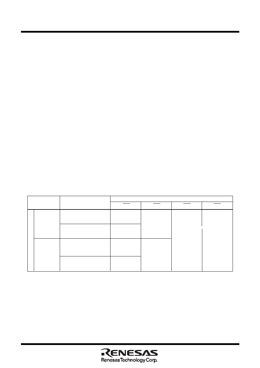
Processor mode
Memory space
expansion mode
Specified
address
range
Memory expansion mode
Normal mode
(PM15,14=0,0)
Chip select signal
CS0
CS1
CS2
CS3
3000016 to
CFFFF16
(640K bytes)
Microprocessor mode
Memory expansion mode
Expansion
mode
(PM15,14=1,1)
2800016 to
2FFFF16
(32K bytes)
0800016 to
27FFF16
(128K bytes)
0400016 to
07FFF16
(16K bytes)
3000016 to
FFFFF16
(832K bytes)
4000016 to
BFFFF16
(512K bytes X 7 +
256K bytes)
2800016 to
3FFFF16
(96K bytes)
Microprocessor mode
4000016 to
FFFFF16
(512K bytes X 8)
Table 1.10.1. External areas specified by the chip select signals
(A product having an internal RAM equal to or less than 15K bytes and a ROM equal to or less than 192K bytes)(Note)
Note :Be sure to set bit 3 (PM13) of processor mode register 1 to “0”.
相关PDF资料 |
PDF描述 |
|---|---|
| M30622MGN-XXXGP | 16-BIT, MROM, 16 MHz, MICROCONTROLLER, PQFP100 |
| M30620FCNFP | 16-BIT, FLASH, 16 MHz, MICROCONTROLLER, PQFP100 |
| M30624MGN-XXXGP | 16-BIT, MROM, 16 MHz, MICROCONTROLLER, PQFP100 |
| M30620SGP | 16-BIT, 16 MHz, MICROCONTROLLER, PQFP100 |
| M30620MA-XXXGP | 16-BIT, MROM, 16 MHz, MICROCONTROLLER, PQFP100 |
相关代理商/技术参数 |
参数描述 |
|---|---|
| M30624FGNGP D3 | 制造商:Renesas Electronics Corporation 功能描述: |
| M30624FGNGP#D3 | 制造商:Renesas Electronics Corporation 功能描述:MCU 16-Bit R8C CISC 256KB Flash 3.3V 100-Pin LQFP 制造商:Renesas Electronics Corporation 功能描述:MCU 16BIT R8C CISC 256KB FLASH 3.3V 100LQFP - Trays |
| M30624FGNGP#D5 | 功能描述:IC M16C MCU FLASH 256K 100LQFP RoHS:否 类别:集成电路 (IC) >> 嵌入式 - 微控制器, 系列:M16C™ M16C/60 标准包装:160 系列:S08 核心处理器:S08 芯体尺寸:8-位 速度:40MHz 连通性:I²C,LIN,SCI,SPI 外围设备:LCD,LVD,POR,PWM,WDT 输入/输出数:53 程序存储器容量:32KB(32K x 8) 程序存储器类型:闪存 EEPROM 大小:- RAM 容量:1.9K x 8 电压 - 电源 (Vcc/Vdd):2.7 V ~ 5.5 V 数据转换器:A/D 12x12b 振荡器型:内部 工作温度:-40°C ~ 105°C 封装/外壳:64-LQFP 包装:托盘 |
| M30624FGNGP#U3 | 功能描述:MCU 3V 256K I-TEMP PB-FREE 100-L RoHS:是 类别:集成电路 (IC) >> 嵌入式 - 微控制器, 系列:M16C™ M16C/60 标准包装:160 系列:S08 核心处理器:S08 芯体尺寸:8-位 速度:40MHz 连通性:I²C,LIN,SCI,SPI 外围设备:LCD,LVD,POR,PWM,WDT 输入/输出数:53 程序存储器容量:32KB(32K x 8) 程序存储器类型:闪存 EEPROM 大小:- RAM 容量:1.9K x 8 电压 - 电源 (Vcc/Vdd):2.7 V ~ 5.5 V 数据转换器:A/D 12x12b 振荡器型:内部 工作温度:-40°C ~ 105°C 封装/外壳:64-LQFP 包装:托盘 |
| M30624FGNGP#U5 | 功能描述:IC M16C MCU FLASH 100LQFP RoHS:是 类别:集成电路 (IC) >> 嵌入式 - 微控制器, 系列:M16C™ M16C/60 标准包装:160 系列:S08 核心处理器:S08 芯体尺寸:8-位 速度:40MHz 连通性:I²C,LIN,SCI,SPI 外围设备:LCD,LVD,POR,PWM,WDT 输入/输出数:53 程序存储器容量:32KB(32K x 8) 程序存储器类型:闪存 EEPROM 大小:- RAM 容量:1.9K x 8 电压 - 电源 (Vcc/Vdd):2.7 V ~ 5.5 V 数据转换器:A/D 12x12b 振荡器型:内部 工作温度:-40°C ~ 105°C 封装/外壳:64-LQFP 包装:托盘 |
发布紧急采购,3分钟左右您将得到回复。