- 您现在的位置:买卖IC网 > PDF目录45017 > M30624FGNGP 16-BIT, FLASH, 16 MHz, MICROCONTROLLER, PQFP100 PDF资料下载
参数资料
| 型号: | M30624FGNGP |
| 元件分类: | 微控制器/微处理器 |
| 英文描述: | 16-BIT, FLASH, 16 MHz, MICROCONTROLLER, PQFP100 |
| 封装: | 14 X 14 MM, 0.50 MM PITCH, PLASTIC, LQFP-100 |
| 文件页数: | 49/248页 |
| 文件大小: | 3871K |
| 代理商: | M30624FGNGP |
第1页第2页第3页第4页第5页第6页第7页第8页第9页第10页第11页第12页第13页第14页第15页第16页第17页第18页第19页第20页第21页第22页第23页第24页第25页第26页第27页第28页第29页第30页第31页第32页第33页第34页第35页第36页第37页第38页第39页第40页第41页第42页第43页第44页第45页第46页第47页第48页当前第49页第50页第51页第52页第53页第54页第55页第56页第57页第58页第59页第60页第61页第62页第63页第64页第65页第66页第67页第68页第69页第70页第71页第72页第73页第74页第75页第76页第77页第78页第79页第80页第81页第82页第83页第84页第85页第86页第87页第88页第89页第90页第91页第92页第93页第94页第95页第96页第97页第98页第99页第100页第101页第102页第103页第104页第105页第106页第107页第108页第109页第110页第111页第112页第113页第114页第115页第116页第117页第118页第119页第120页第121页第122页第123页第124页第125页第126页第127页第128页第129页第130页第131页第132页第133页第134页第135页第136页第137页第138页第139页第140页第141页第142页第143页第144页第145页第146页第147页第148页第149页第150页第151页第152页第153页第154页第155页第156页第157页第158页第159页第160页第161页第162页第163页第164页第165页第166页第167页第168页第169页第170页第171页第172页第173页第174页第175页第176页第177页第178页第179页第180页第181页第182页第183页第184页第185页第186页第187页第188页第189页第190页第191页第192页第193页第194页第195页第196页第197页第198页第199页第200页第201页第202页第203页第204页第205页第206页第207页第208页第209页第210页第211页第212页第213页第214页第215页第216页第217页第218页第219页第220页第221页第222页第223页第224页第225页第226页第227页第228页第229页第230页第231页第232页第233页第234页第235页第236页第237页第238页第239页第240页第241页第242页第243页第244页第245页第246页第247页第248页
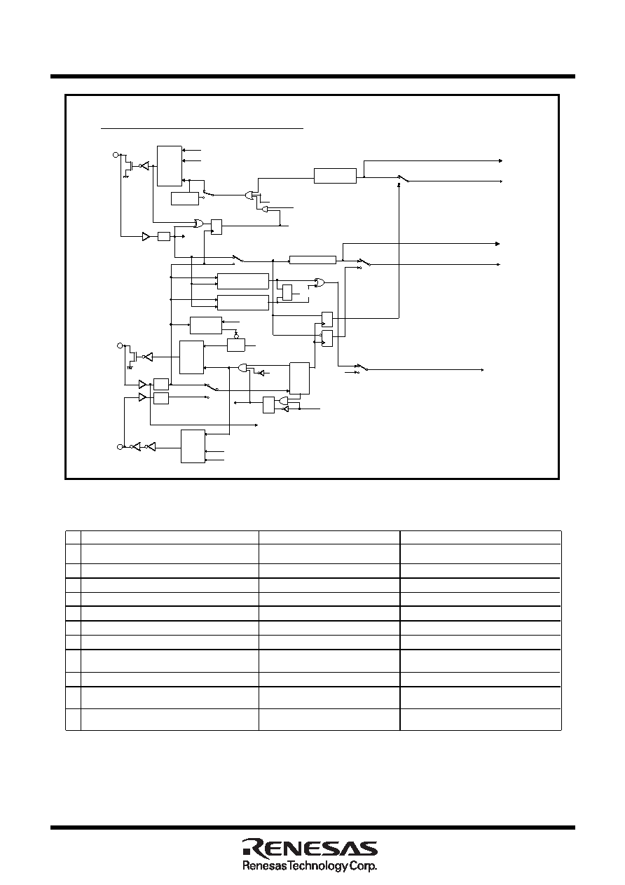
UART2 Special Mode Register
141
Mitsubishi microcomputers
M16C / 62N Group
SINGLE-CHIP 16-BIT CMOS MICROCOMPUTER
Function
Normal mode
I2C mode (Note 1)
Factor of interrupt number 15 (Note 2)
UART2 transmission
No acknowledgment detection (NACK)
Factor of interrupt number 16 (Note 2)
UART2 reception
Start condition detection or stop
condition detection
UART2 transmission output delay
Not delayed
Delayed (digital delay)
P70 at the time when UART2 is in use
TxD2 (output)
SDA (input/output) (Note 3)
P71 at the time when UART2 is in use
RxD2 (input)
SCL (input/output)
P72 at the time when UART2 is in use
CLK2
P72
DMA1 factor at the time when 1 1 0 1 is assigned
to the DMA request factor selection bits
UART2 reception
Acknowledgment detection (ACK)
Noise filter width
15ns
200ns
Reading P71
Reading the terminal when 0 is
assigned to the direction register
Reading the terminal regardless of the
value of the direction register
1
2
3
4
5
6
7
8
9
Note 1: Make the settings given below when I2C mode is in use.
Set 0 1 0 in bits 2, 1, 0 of the UART2 transmission/reception mode register.
Disable the RTS/CTS function. Choose the MSB First function.
Note 2: Follow the steps given below to switch from a factor to another.
1. Disable the interrupt of the corresponding number.
2. Switch from a factor to another.
3. Reset the interrupt request flag of the corresponding number.
4. Set an interrupt level of the corresponding number.
Note 3: Set an initial value of SDA transmission output when serial I/O is invalid.
Factor of interrupt number 10 (Note 2)
Bus collision detection
Acknowledgment detection (ACK)
10
Initial value of UART2 output
H level (when 0 is assigned to
the CLK polarity select bit)
The value set in latch P70 when the port is
selected
11
Table 1.17.9. Features in I2C mode
P70/TxD2/SDA
P71/RxD2/SCL
CLK
control
P72/CLK2
Falling edge
detection
UART2 reception/ACK interrupt
request, DMA1 request
To DMA0, DMA1
To DMA0
2
P70 through P72 conforming to the simplified I C bus
I/O
Timer
UART2
Timer
UART2
IICM=0
or IICM2=1
IICM=1
and IICM2=0
SDHI
Noize
Filter
Timer
UART2
I/O
D
T
Q
D
T
Q
D
T
Q
NACK
ACK
UART2
IICM=1
IICM=0
IICM=1
IICM=0
S
R
Q
IICM=1
IICM=0
I/O
R
Q
ALS
SDDS=0
or DL=000
SDDS=1 and
DL
≠000
SWC2
Falling edge of 9 bit
SWC
IICM=1
and IICM2=0
IICM=0
or IICM2=1
Selector
Noize
Filter
Noize
Filter
*
With IICM set to 1, the port terminal is to be readable
even if 1 is assigned to P7 1 of the direction register.
Port reading
External clock
Internal clock
9th pulse
Bus collision
detection
Bus collision/start, stop condition
detection interrupt request
UART2 transmission/
NACK interrupt request
Start condition
detection
Stop condition
detection
L-synchronous
output enabling
bit
(Port P71 output data latch)
Data bus
Reception register
Bus busy
Transmission
register
Arbitration
Digital delay
(Divider)
Figure 1.17.27. Functional block diagram for I2C mode
相关PDF资料 |
PDF描述 |
|---|---|
| M30622MGN-XXXGP | 16-BIT, MROM, 16 MHz, MICROCONTROLLER, PQFP100 |
| M30620FCNFP | 16-BIT, FLASH, 16 MHz, MICROCONTROLLER, PQFP100 |
| M30624MGN-XXXGP | 16-BIT, MROM, 16 MHz, MICROCONTROLLER, PQFP100 |
| M30620SGP | 16-BIT, 16 MHz, MICROCONTROLLER, PQFP100 |
| M30620MA-XXXGP | 16-BIT, MROM, 16 MHz, MICROCONTROLLER, PQFP100 |
相关代理商/技术参数 |
参数描述 |
|---|---|
| M30624FGNGP D3 | 制造商:Renesas Electronics Corporation 功能描述: |
| M30624FGNGP#D3 | 制造商:Renesas Electronics Corporation 功能描述:MCU 16-Bit R8C CISC 256KB Flash 3.3V 100-Pin LQFP 制造商:Renesas Electronics Corporation 功能描述:MCU 16BIT R8C CISC 256KB FLASH 3.3V 100LQFP - Trays |
| M30624FGNGP#D5 | 功能描述:IC M16C MCU FLASH 256K 100LQFP RoHS:否 类别:集成电路 (IC) >> 嵌入式 - 微控制器, 系列:M16C™ M16C/60 标准包装:160 系列:S08 核心处理器:S08 芯体尺寸:8-位 速度:40MHz 连通性:I²C,LIN,SCI,SPI 外围设备:LCD,LVD,POR,PWM,WDT 输入/输出数:53 程序存储器容量:32KB(32K x 8) 程序存储器类型:闪存 EEPROM 大小:- RAM 容量:1.9K x 8 电压 - 电源 (Vcc/Vdd):2.7 V ~ 5.5 V 数据转换器:A/D 12x12b 振荡器型:内部 工作温度:-40°C ~ 105°C 封装/外壳:64-LQFP 包装:托盘 |
| M30624FGNGP#U3 | 功能描述:MCU 3V 256K I-TEMP PB-FREE 100-L RoHS:是 类别:集成电路 (IC) >> 嵌入式 - 微控制器, 系列:M16C™ M16C/60 标准包装:160 系列:S08 核心处理器:S08 芯体尺寸:8-位 速度:40MHz 连通性:I²C,LIN,SCI,SPI 外围设备:LCD,LVD,POR,PWM,WDT 输入/输出数:53 程序存储器容量:32KB(32K x 8) 程序存储器类型:闪存 EEPROM 大小:- RAM 容量:1.9K x 8 电压 - 电源 (Vcc/Vdd):2.7 V ~ 5.5 V 数据转换器:A/D 12x12b 振荡器型:内部 工作温度:-40°C ~ 105°C 封装/外壳:64-LQFP 包装:托盘 |
| M30624FGNGP#U5 | 功能描述:IC M16C MCU FLASH 100LQFP RoHS:是 类别:集成电路 (IC) >> 嵌入式 - 微控制器, 系列:M16C™ M16C/60 标准包装:160 系列:S08 核心处理器:S08 芯体尺寸:8-位 速度:40MHz 连通性:I²C,LIN,SCI,SPI 外围设备:LCD,LVD,POR,PWM,WDT 输入/输出数:53 程序存储器容量:32KB(32K x 8) 程序存储器类型:闪存 EEPROM 大小:- RAM 容量:1.9K x 8 电压 - 电源 (Vcc/Vdd):2.7 V ~ 5.5 V 数据转换器:A/D 12x12b 振荡器型:内部 工作温度:-40°C ~ 105°C 封装/外壳:64-LQFP 包装:托盘 |
发布紧急采购,3分钟左右您将得到回复。