- 您现在的位置:买卖IC网 > PDF目录68607 > M30625FGNGP 16-BIT, FLASH, 16 MHz, MICROCONTROLLER, PQFP80 PDF资料下载
参数资料
| 型号: | M30625FGNGP |
| 元件分类: | 微控制器/微处理器 |
| 英文描述: | 16-BIT, FLASH, 16 MHz, MICROCONTROLLER, PQFP80 |
| 封装: | 14 X 14 MM, 0.65 MM PITCH, PLASTIC, QFP-80 |
| 文件页数: | 72/212页 |
| 文件大小: | 2676K |
| 代理商: | M30625FGNGP |
第1页第2页第3页第4页第5页第6页第7页第8页第9页第10页第11页第12页第13页第14页第15页第16页第17页第18页第19页第20页第21页第22页第23页第24页第25页第26页第27页第28页第29页第30页第31页第32页第33页第34页第35页第36页第37页第38页第39页第40页第41页第42页第43页第44页第45页第46页第47页第48页第49页第50页第51页第52页第53页第54页第55页第56页第57页第58页第59页第60页第61页第62页第63页第64页第65页第66页第67页第68页第69页第70页第71页当前第72页第73页第74页第75页第76页第77页第78页第79页第80页第81页第82页第83页第84页第85页第86页第87页第88页第89页第90页第91页第92页第93页第94页第95页第96页第97页第98页第99页第100页第101页第102页第103页第104页第105页第106页第107页第108页第109页第110页第111页第112页第113页第114页第115页第116页第117页第118页第119页第120页第121页第122页第123页第124页第125页第126页第127页第128页第129页第130页第131页第132页第133页第134页第135页第136页第137页第138页第139页第140页第141页第142页第143页第144页第145页第146页第147页第148页第149页第150页第151页第152页第153页第154页第155页第156页第157页第158页第159页第160页第161页第162页第163页第164页第165页第166页第167页第168页第169页第170页第171页第172页第173页第174页第175页第176页第177页第178页第179页第180页第181页第182页第183页第184页第185页第186页第187页第188页第189页第190页第191页第192页第193页第194页第195页第196页第197页第198页第199页第200页第201页第202页第203页第204页第205页第206页第207页第208页第209页第210页第211页第212页
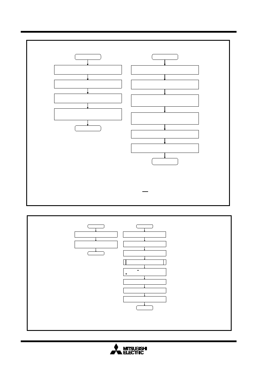
CPU Rewrite Mode (Flash Memory Version)
163
Mitsubishi microcomputers
M16C / 62N Group (80-pin)
SINGLE-CHIP 16-BIT CMOS MICROCOMPUTER
End
Start
Execute read array command or reset flash
memory by setting flash memory reset bit (by
writing “1” and then “0” in succession) (Note 3)
Single-chip mode, or boot mode
Set processor mode register (Note 1)
Using software command execute erase,
program, or other operation
(Set lock bit disable bit as required)
Jump to transferred control program in RAM
(Subsequent operations are executed by control
program in this RAM)
Transfer CPU rewrite mode control
program to internal RAM
(Boot mode only)
Write “0” to user ROM area select bit (Note 4)
Write “0” to CPU rewrite mode select bit
(Boot mode only)
Set user ROM area select bit to “1”
Set CPU rewrite mode select bit to “1” (by
writing “0” and then “1” in succession)(Note 2)
*1
Program in ROM
Program in RAM
Note 1: During CPU rewrite mode, set the BCLK as shown below using the main clock divide ratio select bit (bit 6
at address 000616 and bits 6 and 7 at address 000716):
6.25 MHz or less when wait bit (bit 7 at address 000516) = “0” (without internal access wait state)
10.0 MHz or less when wait bit (bit 7 at address 000516) = “1” (with internal access wait state)
Note 2: For CPU rewrite mode select bit to be set to “1”, the user needs to write a “0” and then a “1” to it in
succession. When it is not this procedure, it is not enacted in “1”. This is necessary to ensure that no
interrupt or DMA transfer will be executed during the interval. Write to this bit only when executing out of
an area other than the internal flash memory. Also only when NMI pin is “H” level.
Note 3: Before exiting the CPU rewrite mode after completing erase or program operation, always be sure to
execute a read array command or reset the flash memory.
Note 4: “1” can be set. However, when this bit is “1”, user ROM area is accessed.
Figure 1.29.2. CPU rewrite mode set/reset flowchart
Figure 1.29.2b. Shifting to the low power dissipation mode flowchart
End
Start
XIN oscillating
Transfer the program to be executed in the low
power dissipation mode, to the internal RAM.
Switch the count source of BCLK.
XIN stop. (Note 2)
Jump to transferred control program in RAM
(Subsequent operations are executed by control
program in this RAM)
Note 1: For flash memory reset bit to be set to “1”, the user needs to write a “0” and then a “1” to it in succession.
When it is not this procedure, it is not enacted in “1”. This is necessary to ensure that no interrupt or DMA
transfer will be executed during the interval.
Note 2: Before the count source for BCLK can be changed from XIN to XCIN or vice versa, the clock to which
the count source is going to be switched must be oscillating stably.
Note 3: Make a waiting time for 10
s by software.
In this waiting time, do not access flash memory.
Wait time until the internal circuit stabilizes (10
s)
(Note 3)
Set flash memory reset bit to “0”
Set flash memory reset bit to “1”
(by writing “0” and then “1” in succession)(Note 1)
*1
Program in ROM
Program in RAM
Process of low power dissipation mode
Wait until the XIN has stabilized
Switch the count source of BCLK (Note 2)
Set CPU rewrite mode select bit to “1”
(by writing “0” and then “1” in succession)
Set CPU rewrite mode select bit to “0”
相关PDF资料 |
PDF描述 |
|---|---|
| M306K7F8LRP | 16-BIT, FLASH, 8 MHz, MICROCONTROLLER, PQFP144 |
| M35052-001FP | 24 X 10 CHARACTERS CRT CHAR DSPL CTLR, PDSO20 |
| MAX6826LUT+T | Dual, Ultra-Low-Voltage SOT23 µP Supervisors with Manual Reset and Watchdog Timer |
| MAX6826MUT+T | Dual, Ultra-Low-Voltage SOT23 µP Supervisors with Manual Reset and Watchdog Timer |
| MAX6826RUT+T | Dual, Ultra-Low-Voltage SOT23 µP Supervisors with Manual Reset and Watchdog Timer |
相关代理商/技术参数 |
参数描述 |
|---|---|
| M30625FGPGP | 制造商:RENESAS 制造商全称:Renesas Technology Corp 功能描述:SINGLE-CHIP 16-BIT CMOS MICROCOMPUTER |
| M30625FGPGP#D5C | 功能描述:IC M16C MCU FLASH 256K 100-LQFP RoHS:否 类别:集成电路 (IC) >> 嵌入式 - 微控制器, 系列:M16C™ M16C/60/62P 产品培训模块:CAN Basics Part-1 CAN Basics Part-2 Electromagnetic Noise Reduction Techniques Part 1 M16C Product Overview Part 1 M16C Product Overview Part 2 标准包装:1 系列:M16C™ M32C/80/87 核心处理器:M32C/80 芯体尺寸:16/32-位 速度:32MHz 连通性:EBI/EMI,I²C,IEBus,IrDA,SIO,UART/USART 外围设备:DMA,POR,PWM,WDT 输入/输出数:121 程序存储器容量:384KB(384K x 8) 程序存储器类型:闪存 EEPROM 大小:- RAM 容量:24K x 8 电压 - 电源 (Vcc/Vdd):3 V ~ 5.5 V 数据转换器:A/D 34x10b,D/A 2x8b 振荡器型:内部 工作温度:-20°C ~ 85°C 封装/外壳:144-LQFP 包装:托盘 产品目录页面:749 (CN2011-ZH PDF) 配用:R0K330879S001BE-ND - KIT DEV RSK M32C/87 |
| M30625FGPGP#U3C | 功能描述:IC M16C MCU FLASH 256K 128LQFP RoHS:是 类别:集成电路 (IC) >> 嵌入式 - 微控制器, 系列:M16C™ M16C/60/62P 产品培训模块:CAN Basics Part-1 CAN Basics Part-2 Electromagnetic Noise Reduction Techniques Part 1 M16C Product Overview Part 1 M16C Product Overview Part 2 标准包装:1 系列:M16C™ M32C/80/87 核心处理器:M32C/80 芯体尺寸:16/32-位 速度:32MHz 连通性:EBI/EMI,I²C,IEBus,IrDA,SIO,UART/USART 外围设备:DMA,POR,PWM,WDT 输入/输出数:121 程序存储器容量:384KB(384K x 8) 程序存储器类型:闪存 EEPROM 大小:- RAM 容量:24K x 8 电压 - 电源 (Vcc/Vdd):3 V ~ 5.5 V 数据转换器:A/D 34x10b,D/A 2x8b 振荡器型:内部 工作温度:-20°C ~ 85°C 封装/外壳:144-LQFP 包装:托盘 产品目录页面:749 (CN2011-ZH PDF) 配用:R0K330879S001BE-ND - KIT DEV RSK M32C/87 |
| M30625FGPGP#U5C | 功能描述:IC M16C MCU FLASH 256K 128LQFP RoHS:是 类别:集成电路 (IC) >> 嵌入式 - 微控制器, 系列:M16C™ M16C/60/62P 产品培训模块:CAN Basics Part-1 CAN Basics Part-2 Electromagnetic Noise Reduction Techniques Part 1 M16C Product Overview Part 1 M16C Product Overview Part 2 标准包装:1 系列:M16C™ M32C/80/87 核心处理器:M32C/80 芯体尺寸:16/32-位 速度:32MHz 连通性:EBI/EMI,I²C,IEBus,IrDA,SIO,UART/USART 外围设备:DMA,POR,PWM,WDT 输入/输出数:121 程序存储器容量:384KB(384K x 8) 程序存储器类型:闪存 EEPROM 大小:- RAM 容量:24K x 8 电压 - 电源 (Vcc/Vdd):3 V ~ 5.5 V 数据转换器:A/D 34x10b,D/A 2x8b 振荡器型:内部 工作温度:-20°C ~ 85°C 封装/外壳:144-LQFP 包装:托盘 产品目录页面:749 (CN2011-ZH PDF) 配用:R0K330879S001BE-ND - KIT DEV RSK M32C/87 |
| M30625FGPGP#U7C | 功能描述:IC M16C MCU FLASH 256K 128LQFP RoHS:是 类别:集成电路 (IC) >> 嵌入式 - 微控制器, 系列:M16C™ M16C/60/62P 产品培训模块:CAN Basics Part-1 CAN Basics Part-2 Electromagnetic Noise Reduction Techniques Part 1 M16C Product Overview Part 1 M16C Product Overview Part 2 标准包装:1 系列:M16C™ M32C/80/87 核心处理器:M32C/80 芯体尺寸:16/32-位 速度:32MHz 连通性:EBI/EMI,I²C,IEBus,IrDA,SIO,UART/USART 外围设备:DMA,POR,PWM,WDT 输入/输出数:121 程序存储器容量:384KB(384K x 8) 程序存储器类型:闪存 EEPROM 大小:- RAM 容量:24K x 8 电压 - 电源 (Vcc/Vdd):3 V ~ 5.5 V 数据转换器:A/D 34x10b,D/A 2x8b 振荡器型:内部 工作温度:-20°C ~ 85°C 封装/外壳:144-LQFP 包装:托盘 产品目录页面:749 (CN2011-ZH PDF) 配用:R0K330879S001BE-ND - KIT DEV RSK M32C/87 |
发布紧急采购,3分钟左右您将得到回复。