- 您现在的位置:买卖IC网 > PDF目录45021 > M3062AFCTFP-B 16-BIT, FLASH, 24 MHz, MICROCONTROLLER, PQFP100 PDF资料下载
参数资料
| 型号: | M3062AFCTFP-B |
| 元件分类: | 微控制器/微处理器 |
| 英文描述: | 16-BIT, FLASH, 24 MHz, MICROCONTROLLER, PQFP100 |
| 封装: | 14 X 20 MM, 0.65 MM PITCH, PLASTIC, QFP-100 |
| 文件页数: | 9/87页 |
| 文件大小: | 919K |
| 代理商: | M3062AFCTFP-B |
第1页第2页第3页第4页第5页第6页第7页第8页当前第9页第10页第11页第12页第13页第14页第15页第16页第17页第18页第19页第20页第21页第22页第23页第24页第25页第26页第27页第28页第29页第30页第31页第32页第33页第34页第35页第36页第37页第38页第39页第40页第41页第42页第43页第44页第45页第46页第47页第48页第49页第50页第51页第52页第53页第54页第55页第56页第57页第58页第59页第60页第61页第62页第63页第64页第65页第66页第67页第68页第69页第70页第71页第72页第73页第74页第75页第76页第77页第78页第79页第80页第81页第82页第83页第84页第85页第86页第87页
M16C/62P Group (M16C/62P, M16C/62PT)
4
8
f
o
4
0
2
,
1
0
p
e
S
0
3
.
2
.
v
e
R
Z
0
3
2
0
-
1
0
B
3
0
J
E
R
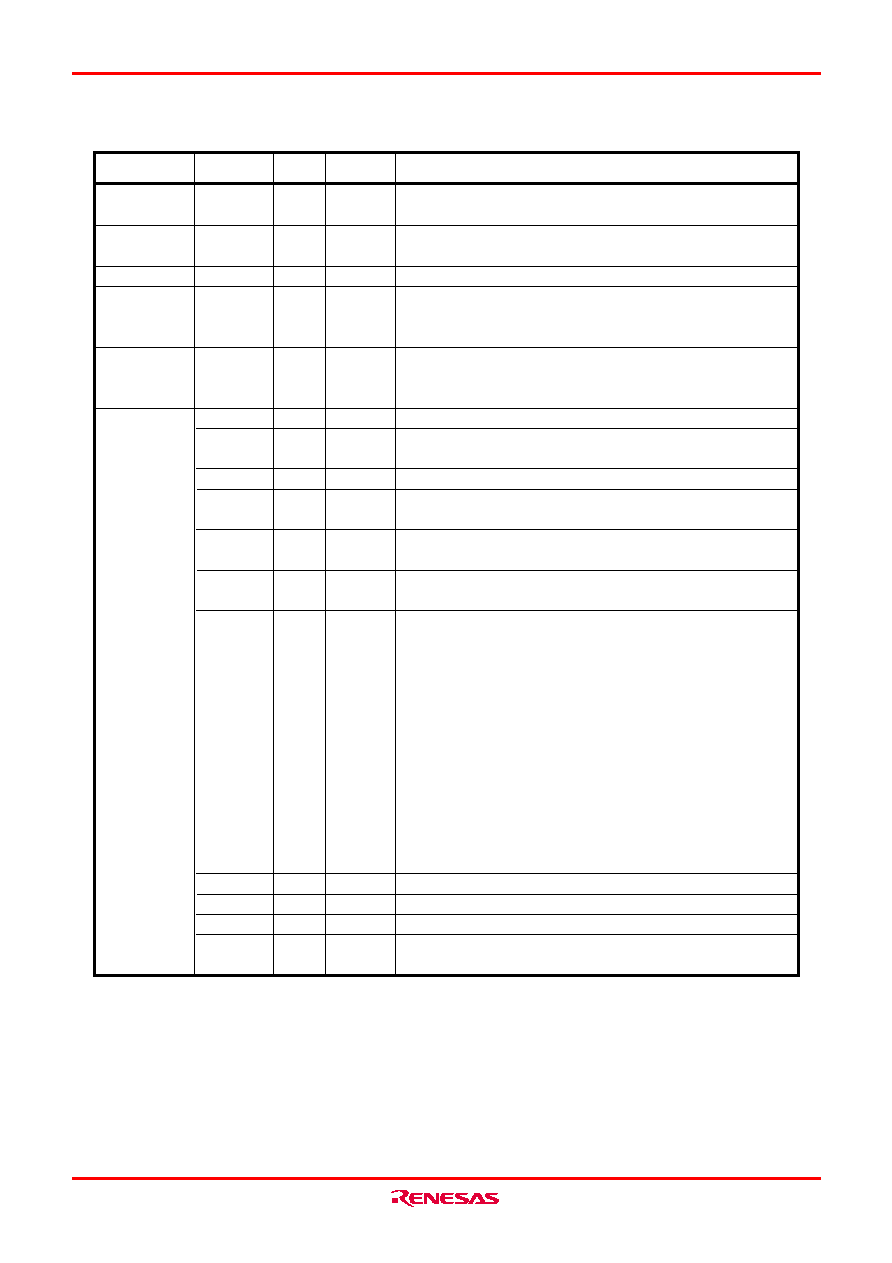
page 17
1. Overview
1.6 Pin Description
Table 1.10 Pin Description (100-pin and 128-pin Version) (1)
Apply 2.7 to 5.5 V to the VCC1 and VCC2 pins and 0 V to the VSS pin. The VCC
apply condition is that VCC1
≥ VCC2.(2)
Applies the power supply for the A/D converter. Connect the AVCC pin to
VCC1. Connect the AVSS pin to VSS.
The microcomputer is in a reset state when applying "L" to the this pin.
Switches processor mode. Connect this pin to VSS to when after a reset to start
up in single-chip mode. Connect this pin to VCC1 to start up in microprocessor
mode.
Switches the data bus in external memory space. The data bus is 16 bits long
when the this pin is held "L" and 8 bits long when the this pin is held "H". Set it
to either one. Connect this pin to VSS when an single-chip mode.
Inputs and outputs data (D0 to D7) when these pins are set as the separate bus.
Inputs and outputs data (D8 to D15) when external 16-bit data bus is set as the
separate bus.
Output address bits (A0 to A19).
Input and output data (D0 to D7) and output address bits (A0 to A7) by time-
sharing when external 8-bit data bus are set as the multiplexed bus.
Input and output data (D0 to D7) and output address bits (A8 to A15) by time-
sharing when external 16-bit data bus are set as the multiplexed bus.
________
Output CS0 to CS3 signals. CS0 to CS3 are chip-select signals to specify an
external space.
________ _________
______ ________
_____
________
_________
_______
______
Output WRL, WRH, (WR, BHE), RD signals. WRL and WRH or BHE and WR
can be switched by program.
________ _________
_____
WRL, WRH and RD are selected
________
The WRL signal becomes "L" by writing data to an even address in an external
memory space.
_________
The WRH signal becomes "L" by writing data to an odd address in an external
memory space.
_____
The RD pin signal becomes "L" by reading data in an external memory space.
______ ________
_____
WR, BHE and RD are selected
______
The WR signal becomes "L" by writing data in an external memory space.
_____
The RD signal becomes "L" by reading data in an external memory space.
________
The BHE signal becomes "L" by accessing an odd address.
______ ________
_____
Select WR, BHE and RD for an external 8-bit data bus.
ALE is a signal to latch the address.
__________
While the HOLD pin is held "L", the microcomputer is placed in a hold state.
_________
In a hold state, HLDA outputs a "L" signal.
________
While applying a "L" signal to the RDY pin, the microcomputer is placed in a wait
state.
VCC1, VCC2
VSS
AVCC
AVSS
____________
RESET
CNVSS
BYTE
D0 to D7
D8 to D15
A0 to A19
A0/D0 to
A7/D7
A1/D0 to
A8/D7
______
CS0 to CS3
________ ______
WRL/WR
_________ ________
WRH/BHE
_____
RD
ALE
__________
HOLD
__________
HLDA
________
RDY
Power supply input
Analog power
supply input
Reset input
CNVSS
External data bus
width select input
Bus control pins(4)
I
I/O
O
I/O
O
I
O
I
-
VCC1
VCC2
Power
Signal Name
Pin Name I/O Type
Description
Supply(3)
I : Input
O : Output
I/O : Input and output
Power Supply : Power supplies which relate to the external bus pins are separated as VCC2, thus they can be inter-
faced using the different voltage as VCC1.
NOTES:
1. In this manual, hereafter, VCC refers to VCC1 unless otherwise noted.
2. In M16C/62PT, apply 2.7 to 5.5 V to the VCC1 and VCC2 pins. Also the apply condition is that VCC1
≥ VCC2.
3. When use VCC1 > VCC2, contacts due to some points or restrictions to be checked.
4. Bus control pins in M16C/62Tcannot be used.
相关PDF资料 |
PDF描述 |
|---|---|
| M3062AFCTGP-U7 | 16-BIT, FLASH, 24 MHz, MICROCONTROLLER, PQFP100 |
| M3062AFCVGP-U7 | 16-BIT, FLASH, 24 MHz, MICROCONTROLLER, PQFP100 |
| M3062JFHTFP-U7 | 16-BIT, FLASH, 24 MHz, MICROCONTROLLER, PQFP100 |
| M3062JFHVFP-U7 | 16-BIT, FLASH, 24 MHz, MICROCONTROLLER, PQFP100 |
| M30622F8PGP-D9 | 16-BIT, FLASH, 24 MHz, MICROCONTROLLER, PQFP100 |
相关代理商/技术参数 |
参数描述 |
|---|---|
| M3062AFCTGP | 制造商:RENESAS 制造商全称:Renesas Technology Corp 功能描述:SINGLE-CHIP 16-BIT CMOS MICROCOMPUTER |
| M3062AFCVFP | 制造商:RENESAS 制造商全称:Renesas Technology Corp 功能描述:SINGLE-CHIP 16-BIT CMOS MICROCOMPUTER |
| M3062AFCVGP | 制造商:RENESAS 制造商全称:Renesas Technology Corp 功能描述:SINGLE-CHIP 16-BIT CMOS MICROCOMPUTER |
| M3062AMCT-XXXFP | 制造商:RENESAS 制造商全称:Renesas Technology Corp 功能描述:SINGLE-CHIP 16-BIT CMOS MICROCOMPUTER |
| M3062AMCT-XXXGP | 制造商:RENESAS 制造商全称:Renesas Technology Corp 功能描述:SINGLE-CHIP 16-BIT CMOS MICROCOMPUTER |
发布紧急采购,3分钟左右您将得到回复。