- 您现在的位置:买卖IC网 > PDF目录45023 > M306N4MCT-XXXFP 16-BIT, MROM, 20 MHz, MICROCONTROLLER, PQFP100 PDF资料下载
参数资料
| 型号: | M306N4MCT-XXXFP |
| 元件分类: | 微控制器/微处理器 |
| 英文描述: | 16-BIT, MROM, 20 MHz, MICROCONTROLLER, PQFP100 |
| 封装: | 14 X 20 MM, 0.65 MM PITCH, PLASTIC, QFP-100 |
| 文件页数: | 37/92页 |
| 文件大小: | 694K |
| 代理商: | M306N4MCT-XXXFP |
第1页第2页第3页第4页第5页第6页第7页第8页第9页第10页第11页第12页第13页第14页第15页第16页第17页第18页第19页第20页第21页第22页第23页第24页第25页第26页第27页第28页第29页第30页第31页第32页第33页第34页第35页第36页当前第37页第38页第39页第40页第41页第42页第43页第44页第45页第46页第47页第48页第49页第50页第51页第52页第53页第54页第55页第56页第57页第58页第59页第60页第61页第62页第63页第64页第65页第66页第67页第68页第69页第70页第71页第72页第73页第74页第75页第76页第77页第78页第79页第80页第81页第82页第83页第84页第85页第86页第87页第88页第89页第90页第91页第92页
Rev.2.40
Aug 25, 2006
page 42 of 88
REJ03B0003-02400
M16C/6N Group (M16C/6N4)
5. Electric Characteristics (T/V-ver.)
Under development
This document is under development and its contents are subject to change.
td(BCLK-AD)
th(BCLK-AD)
th(RD-AD)
th(WR-AD)
td(BCLK-CS)
th(BCLK-CS)
td(BCLK-ALE)
th(BCLK-ALE)
td(BCLK-RD)
th(BCLK-RD)
td(BCLK-WR)
th(BCLK-WR)
td(BCLK-DB)
th(BCLK-DB)
td(DB-WR)
th(WR-DB)
td(BCLK-HLDA)
ns
Address output delay time
Address output hold time (in relation to BCLK)
Address output hold time (in relation to RD)
Address output hold time (in relation to WR)
Chip select output delay time
Chip select output hold time (in relation to BCLK)
ALE signal output delay time
ALE signal output hold time
RD signal output delay time
RD signal output hold time
WR signal output delay time
WR signal output hold time
Data output delay time (in relation to BCLK)
Data output hold time (in relation to BCLK)
(3)
Data output delay time (in relation to WR)
Data output hold time (in relation to WR)
(3)
__________
HLDA output delay time
Symbol
Parameter
Min.
Standard
Unit
Max.
4
0
(NOTE 1)
4
–4
0
4
(NOTE 2)
(NOTE 1)
Switching Characteristics
(Referenced to VCC = 5 V, VSS = 0 V, at Topr = –40 to 85 °C unless otherwise specified)
Table 5.24 Memory Expansion Mode and Microprocessor Mode (for 1- to 3-wait setting and external area access)
25
15
25
40
NOTES:
1. Calculated according to the BCLK frequency as follows:
0.5
109
f(BCLK)
– 10 [ns]
2. Calculated according to the BCLK frequency as follows:
(n – 0.5)
109
n is “1” for 1-wait setting, “2” for 2-wait setting and “3” for 3-wait setting.
f(BCLK)
– 40 [ns]
When n = 1, f(BCLK) is 12.5 MHz or less.
3. This standard value shows the timing when the
output is off, and does not show hold time of
data bus.
Hold time of data bus varies with capacitor volume
and pull-up (pull-down) resistance value.
Hold time of data bus is expressed in
t = – CR
ln (1 – VOL / VCC)
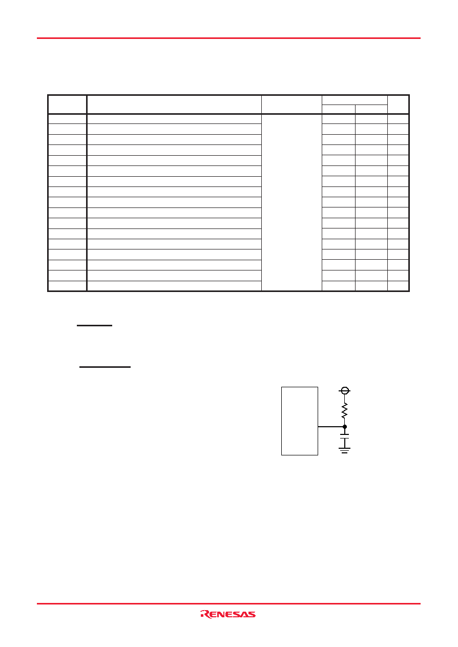
by a circuit of the right figure.
For example, when VOL = 0.2 VCC, C = 30 pF,
R =1 k
, hold time of output “L” level is
t = – 30 pF
1 k ln (1 – 0.2 VCC / VCC) = 6.7 ns.
DBi
R
C
Measuring
Condition
Figure 5.2
VCC = 5 V
相关PDF资料 |
PDF描述 |
|---|---|
| M306N4FCGP | 16-BIT, FLASH, 20 MHz, MICROCONTROLLER, PQFP100 |
| M306N4FGVFP | 16-BIT, FLASH, 20 MHz, MICROCONTROLLER, PQFP100 |
| M306N5FCVFP | 16-BIT, FLASH, 20 MHz, MICROCONTROLLER, PQFP100 |
| M306N5MCV-XXXFP | 16-BIT, MROM, 20 MHz, MICROCONTROLLER, PQFP100 |
| M306N5FCGP | 16-BIT, FLASH, 24 MHz, MICROCONTROLLER, PQFP100 |
相关代理商/技术参数 |
参数描述 |
|---|---|
| M306N4MCT-XXXGP | 制造商:RENESAS 制造商全称:Renesas Technology Corp 功能描述:Renesas MCU |
| M306N4MCV-XXXFP | 制造商:RENESAS 制造商全称:Renesas Technology Corp 功能描述:Renesas MCU |
| M306N4MCV-XXXGP | 制造商:RENESAS 制造商全称:Renesas Technology Corp 功能描述:Renesas MCU |
| M306N4MC-XXXGP | 制造商:RENESAS 制造商全称:Renesas Technology Corp 功能描述:Renesas MCU |
| M306N4MGT-XXXFP | 制造商:RENESAS 制造商全称:Renesas Technology Corp 功能描述:Renesas MCU |
发布紧急采购,3分钟左右您将得到回复。