- 您现在的位置:买卖IC网 > PDF目录383294 > M312L2920BTS-CAA (SAMSUNG SEMICONDUCTOR CO. LTD.) DDR SDRAM Registered Module PDF资料下载
参数资料
| 型号: | M312L2920BTS-CAA |
| 厂商: | SAMSUNG SEMICONDUCTOR CO. LTD. |
| 英文描述: | DDR SDRAM Registered Module |
| 中文描述: | DDR SDRAM的注册模块 |
| 文件页数: | 9/23页 |
| 文件大小: | 258K |
| 代理商: | M312L2920BTS-CAA |
DDR SDRAM
512MB, 1GB, 2GB TSOP Registered DIMM
Revison 1.0 December, 2003
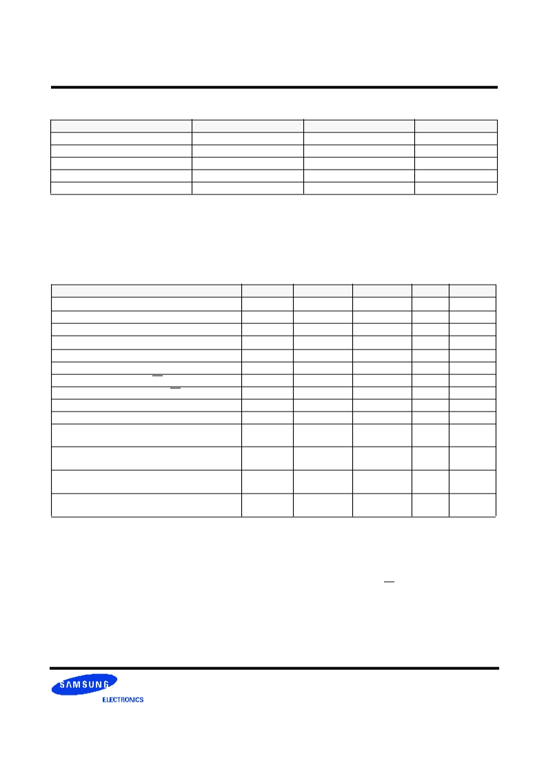
Absolute Maximum Ratings
Parameter
Symbol
Value
Unit
Voltage on any pin relative to Vss
V
IN
, V
OUT
-0.5 ~ 3.6
V
Voltage on V
DD
supply relative to Vss
V
DD,
V
DDQ
-1.0 ~ 3.6
V
Storage temperature
T
STG
-55 ~ +150
C
Power dissipation
P
D
1.5 * # of component
W
Short circuit current
I
OS
50
mA
Permanent device damage may occur if ABSOLUTE MAXIMUM RATINGS are exceeded.
Functional operation should be restricted to recommended operating condition.
Exposure to higher than recommended voltage for extended periods of time could affect device reliability.
Note :
Power & DC Operating Conditions (SSTL_2 In/Out)
Notes :
1. Includes
25mV margin for DC offset on V
REF
, and a combined total of
50mV margin for all AC noise and DC offset on
V
REF
, bandwidth limited to 20MHz. The DRAM must accommodate DRAM current spikes on V
REF
and internal DRAM noise
coupled to V
REF
, both of which may result in V
REF
noise. V
REF
should be de-coupled with an inductance of
3nH.
2. V
TT
is not applied directly to the device. V
TT
is a system supply for signal termination resistors, is expected to be set equal to
V
REF
, and must track variations in the DC level of V
REF
3. V
ID
is the magnitude of the difference between the input level on CK and the input level on CK.
4. These parameters should be tested at the pin on actual components and may be checked at either the pin or the pad in
simulation. The AC and DC input specifications are relative to a VREF envelop that has been bandwidth limited to 200MHz.
Recommended operating conditions (Voltage referenced to V
SS
=0V, T
A
=0 to 70
C)
Parameter
Symbol
Min
Max
Unit
Note
Supply voltage(for device with a nominal V
DD
of 2.5V)
V
DD
2.3
2.7
I/O Supply voltage
V
DDQ
2.3
2.7
V
I/O Reference voltage
V
REF
VDDQ/2-50mV
VDDQ/2+50mV
V
1
I/O Termination voltage(system)
V
TT
V
REF
-0.04
V
REF
+0.04
V
2
Input logic high voltage
V
IH
(DC)
V
REF
+0.15
V
DDQ
+0.3
V
4
Input logic low voltage
V
IL
(DC)
-0.3
V
REF
-0.15
V
4
Input Voltage Level, CK and CK inputs
V
IN
(DC)
-0.3
V
DDQ
+0.3
V
Input Differential Voltage, CK and CK inputs
V
ID
(DC)
0.3
V
DDQ
+0.6
V
3
Input leakage current
I
I
-2
2
uA
Output leakage current
I
OZ
-5
5
uA
Output High Current(Normal strengh driver)
;V
OUT
= V
TT
+ 0.84V
I
OH
-16.8
mA
Output High Current(Normal strengh driver)
;V
OUT
= V
TT
- 0.84V
I
OL
16.8
mA
Output High Current(Half strengh driver)
;V
OUT
=
V
TT
+ 0.45V
I
OH
-9
mA
Output High Current(Half strengh driver)
;V
OUT
= V
TT
- 0.45V
I
OL
9
mA
相关PDF资料 |
PDF描述 |
|---|---|
| M312L2923BTS-A2 | DDR SDRAM Registered Module |
| M312L2923BTS-CAA | DDR SDRAM Registered Module |
| M383L2923BTS-A2 | DDR SDRAM Registered Module |
| M312L2920BG0-CB3 | DDR SDRAM Registered Module |
| M312L5628BT0-A2 | DDR SDRAM Registered Module |
相关代理商/技术参数 |
参数描述 |
|---|---|
| M312L2920CZ3-CB300 | 制造商:Samsung Semiconductor 功能描述:512MSDDDR_MDDR SDRAM MODULX72BOC(LF) - Bulk |
| M312L2920DUS | 制造商:SAMSUNG 制造商全称:Samsung semiconductor 功能描述:DDR SDRAM Product Guide |
| M312L2923BG0-A2 | 制造商:SAMSUNG 制造商全称:Samsung semiconductor 功能描述:DDR SDRAM Registered Module |
| M312L2923BG0-B0 | 制造商:SAMSUNG 制造商全称:Samsung semiconductor 功能描述:DDR SDRAM Registered Module |
| M312L2923BG0-CB3 | 制造商:SAMSUNG 制造商全称:Samsung semiconductor 功能描述:DDR SDRAM Registered Module |
发布紧急采购,3分钟左右您将得到回复。