- 您现在的位置:买卖IC网 > PDF目录383294 > M312L2923BTS-CAA (SAMSUNG SEMICONDUCTOR CO. LTD.) DDR SDRAM Registered Module PDF资料下载
参数资料
| 型号: | M312L2923BTS-CAA |
| 厂商: | SAMSUNG SEMICONDUCTOR CO. LTD. |
| 英文描述: | DDR SDRAM Registered Module |
| 中文描述: | DDR SDRAM的注册模块 |
| 文件页数: | 12/23页 |
| 文件大小: | 258K |
| 代理商: | M312L2923BTS-CAA |
DDR SDRAM
512MB, 1GB, 2GB TSOP Registered DIMM
Revison 1.0 December, 2003
Note :
1. VID is the magnitude of the difference between the input level on CK and the input on CK.
2. The value of V
IX
is expected to equal 0.5*V
DDQ
of the transmitting device and must track variations in the DC level of the same.
3. These parameters should be tested at the pim on actual components and may be checked at either the pin or the pad in
simulation. the AC and DC input specificatims are refation to a Vref envelope that has been bandwidth limited 20MHz.
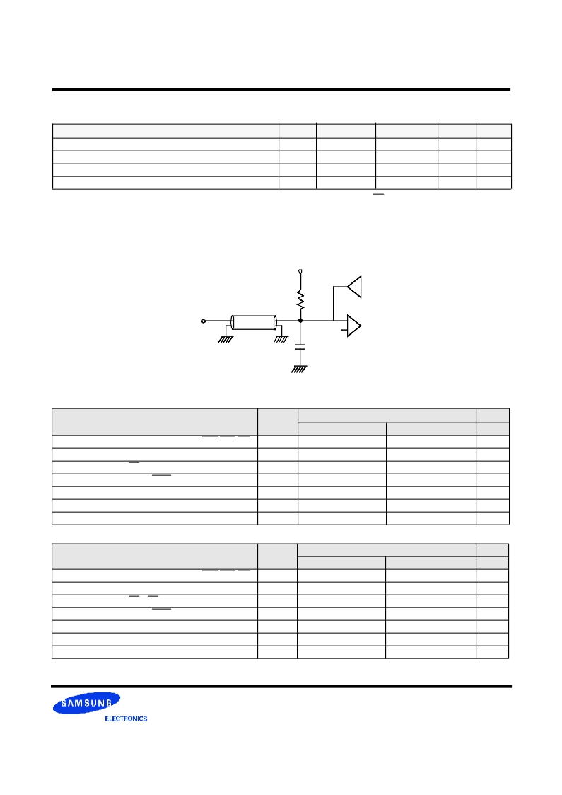
Output Load Circuit (SSTL_2)
Output
Z0=50
C
LOAD
=30pF
=0.5*V
DDQ
R
T
=50
V
tt
=0.5*V
DDQ
Input/Output Capacitance
(VDD=2.5V, VDDQ=2.5V, TA= 25
C, f=1MHz)
Parameter
Symbol
M383(12)L6523BTS, M383(12)L2920BTS
Unit
Min
Max
Input capacitance(A0 ~ A12, BA0 ~ BA1,RAS,CAS,WE )
CIN1
9
11
pF
Input capacitance(CKE0)
CIN2
9
11
pF
Input capacitance( CS0)
CIN3
9
11
pF
Input capacitance( CLK0, CLK0 )
CIN4
11
12
pF
Input capacitance(DM0~DM8)
CIN5
10
11
pF
Data & DQS input/output capacitance(DQ0~DQ63)
Cout1
10
11
pF
Data input/output capacitance (CB0~CB7)
Cout2
10
11
pF
Parameter
Symbol
M383(12)L2923BTS, M383(12)L5628BT1(0)
Unit
Min
Max
Input capacitance(A0 ~ A12, BA0 ~ BA1,RAS,CAS,WE )
CIN1
9
11
pF
Input capacitance(CKE0,CKE1)
CIN2
9
11
pF
Input capacitance( CS0, CS1)
CIN3
9
11
pF
Input capacitance( CLK0, CLK0 )
CIN4
11
12
pF
Input capacitance(DM0~DM8)
CIN5
14
16
pF
Data & DQS input/output capacitance(DQ0~DQ63)
Cout1
14
16
pF
Data input/output capacitance (CB0~CB7)
Cout2
14
16
pF
AC Operating Conditions
Parameter/Condition
Symbol
Min
Max
Unit
Note
Input High (Logic 1) Voltage, DQ, DQS and DM signals
VIH(AC)
VREF + 0.31
V
3
Input Low (Logic 0) Voltage, DQ, DQS and DM signals.
VIL(AC)
VREF - 0.31
V
3
Input Differential Voltage, CK and CK inputs
VID(AC)
0.7
VDDQ+0.6
V
1
Input Crossing Point Voltage, CK and CK inputs
VIX(AC)
0.5*VDDQ-0.2
0.5*VDDQ+0.2
V
2
V
REF
相关PDF资料 |
PDF描述 |
|---|---|
| M383L2923BTS-A2 | DDR SDRAM Registered Module |
| M312L2920BG0-CB3 | DDR SDRAM Registered Module |
| M312L5628BT0-A2 | DDR SDRAM Registered Module |
| M312L5628BT0-CAA | DDR SDRAM Registered Module |
| M312L6523BTS-A2 | DDR SDRAM Registered Module |
相关代理商/技术参数 |
参数描述 |
|---|---|
| M312L2923CZ3-CB300 | 制造商:Samsung Semiconductor 功能描述:512MSDDDR_MDDR SDRAM MODULX72BOC(LF) - Bulk |
| M312L2923CZ3-CB3E0 | 制造商:Samsung Semiconductor 功能描述:512MSDDDR_MDDR SDRAM MODULX72BOC(LF) - Bulk |
| M312L2923DZ3 | 制造商:SAMSUNG 制造商全称:Samsung semiconductor 功能描述:DDR SDRAM Product Guide |
| M312L2923FH3-CCC00 | 制造商:Samsung SDI 功能描述: |
| M312L3223ETS | 制造商:SAMSUNG 制造商全称:Samsung semiconductor 功能描述:DDR SDRAM Registered Module |
发布紧急采购,3分钟左右您将得到回复。