- 您现在的位置:买卖IC网 > PDF目录67761 > M34283G2GP 4-BIT, MROM, 4 MHz, MICROCONTROLLER, PDSO20 PDF资料下载
参数资料
| 型号: | M34283G2GP |
| 元件分类: | 微控制器/微处理器 |
| 英文描述: | 4-BIT, MROM, 4 MHz, MICROCONTROLLER, PDSO20 |
| 封装: | 4.40 X 6.50 MM, 0.65 MM PITCH, PLASTIC, LSSOP-20 |
| 文件页数: | 18/41页 |
| 文件大小: | 441K |
| 代理商: | M34283G2GP |
第1页第2页第3页第4页第5页第6页第7页第8页第9页第10页第11页第12页第13页第14页第15页第16页第17页当前第18页第19页第20页第21页第22页第23页第24页第25页第26页第27页第28页第29页第30页第31页第32页第33页第34页第35页第36页第37页第38页第39页第40页第41页
Rev.1.01
Mar 20, 2006
page 23 of 62
REJ03B0109-0101
4283 Group
LIST OF PRECAUTIONS
Noise and latch-up prevention
Connect a capacitor on the following condition to prevent noise
and latch-up;
connect a bypass capacitor (approx. 0.01
F) between pins
VDD and VSS at the shortest distance,
equalize its wiring in width and length, and
use the thickest wire.
Port E2 is also uesd as VPP pin. Connect this pin to VSS
through the resistor about 5k
which is assigned to E2/VPP
pin as close as possible at the shortest distance.
Register initial values 1
The initial value of the following registers are undefined after
system is released from reset. After system is released from
reset, set initial values.
Register D (3 bits)
Register E (8 bits)
Register initial values 2
The initial value of the following registers are undefined at RAM
backup. After system is returned from RAM back-up, set initial
values.
Register X (4 bits)
Register Y (4 bits)
Register D (3 bits)
Register E (8 bits)
Stack registers (SKS)
Stack registers (SKs) are four identical registers, so that
subroutines can be nested up to 4 levels. However, one of
stack registers is used respectively when using an interrupt
service routine and when executing a table reference
instruction. Accordingly, be careful not to over the stack when
performing these operations together.
Notes on unused pins
Timer
Count source
Stop timer 1 or timer 2 counting to change its count source.
Reading the count value
Stop timer 1 or 2 counting and then execute the data read
instruction (TAB1, TAB2) to read its data.
Watchdog timer
Be sure that the timing to execute the WRST instruction in
order to operate WDT efficiently.
Writing to reload register R1
When writing data to reload register R1 while timer 1 is
operating, avoid a timing when timer 1 underflows.
Timer 1 count operation
When the bit 5 of the watchdog timer (WDT) is selected as
the timer 1 count source, the error of maximum ± 256
s
(at the minimum instruction execution time : 8
s) is
generated from timer 1 start until timer 1 underflow. When
programming, be careful about this error.
Stop of timer 2
Avoid a timing when timer 2 underflows to stop timer 2.
Writing to reload register R2H
When writing data to reload register R2H while timer 2 is
operating, avoid a timing when timer underflows.
Timer 2 carrier wave output function
When to expand “H” interval of carrier wave is valid, set “1”
or more to reload register R2H.
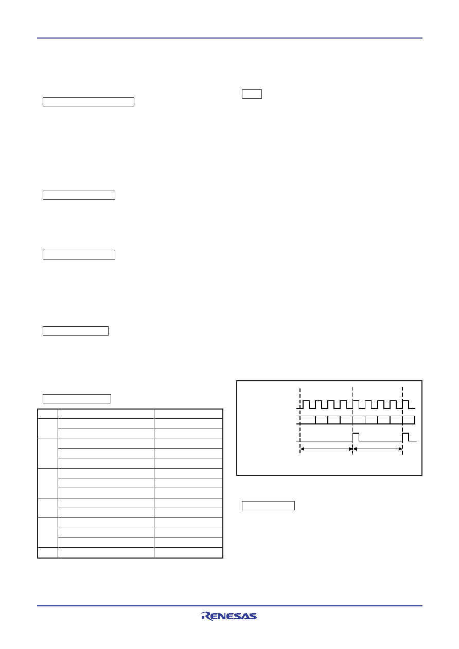
Timer 1 and timer 2 carrier wave output function
Count starts from the rising edge in Fig. 29 after the first
falling edge of the count source, after timer 1 and timer 2
operations start ① in Fig. 29.
Time to first underflow ③ in Fig. 29 is different from time
among next underflow ④ in Fig. 29 by the timing to start the
timer and count source operations after count starts.
Pin
D0–D3
D4–D7
E0, E1
E2
G0–G3
CARR
Connection
Open.
Connect to VDD.
Open (Set the output latch to “1” ).
Open (Set the output latch to “0” ).
Connect to VDD.
Open (Set the output latch to “1” ).
Open (Set the output latch to “0” ).
Connect to VDD.
Open.
Connect to VSS.
Open (Set the output latch to “1” ).
Open (Set the output latch to “0” ).
Connect to VDD.
Open.
Usage condition
Pull-down transistor OFF.
(Note when connecting to VSS and VDD)
Connect the unused pins to VSS and VDD at the shortest
distance and use the thick wire against noise.
Fig. 29 Count start time and count time when operation
starts (T1, T2)
3
21
032
103
→
Timer start
Count source
Timer value
Timer underflow signal
Program counter
Make sure that the program counter does not specify after the
last page of the built-in ROM.
相关PDF资料 |
PDF描述 |
|---|---|
| M34283G2-XXXGP | 4-BIT, MROM, 4 MHz, MICROCONTROLLER, PDSO20 |
| M34502E4FP | 4-BIT, OTPROM, MICROCONTROLLER, PDSO24 |
| M34502M4-XXXFP | 4-BIT, MROM, MICROCONTROLLER, PDSO24 |
| M34502M2-XXXFP | 4-BIT, MROM, MICROCONTROLLER, PDSO24 |
| M34508G4GP | 4-BIT, MROM, 6 MHz, MICROCONTROLLER, PDSO20 |
相关代理商/技术参数 |
参数描述 |
|---|---|
| M34283G2GP#U1 | 制造商:Renesas Electronics Corporation 功能描述:MICROCONTROLLER |
| M34283G2-XXXGP | 制造商:RENESAS 制造商全称:Renesas Technology Corp 功能描述:SINGLE-CHIP 4-BIT CMOS MICROCOMPUTER |
| M34286 | 制造商:RENESAS 制造商全称:Renesas Technology Corp 功能描述:SINGLE-CHIP 4-BIT CMOS MICROCOMPUTER |
| M34286G2GP | 制造商:RENESAS 制造商全称:Renesas Technology Corp 功能描述:SINGLE-CHIP 4-BIT CMOS MICROCOMPUTER |
| M34286G2GP#U0 | 功能描述:MCU 1.8/3.6V 2KB ROM 20-LSSOP RoHS:是 类别:集成电路 (IC) >> 嵌入式 - 微控制器, 系列:720/4500 标准包装:38 系列:Encore!® XP® 核心处理器:eZ8 芯体尺寸:8-位 速度:5MHz 连通性:IrDA,UART/USART 外围设备:欠压检测/复位,LED,POR,PWM,WDT 输入/输出数:16 程序存储器容量:4KB(4K x 8) 程序存储器类型:闪存 EEPROM 大小:- RAM 容量:1K x 8 电压 - 电源 (Vcc/Vdd):2.7 V ~ 3.6 V 数据转换器:- 振荡器型:内部 工作温度:-40°C ~ 105°C 封装/外壳:20-SOIC(0.295",7.50mm 宽) 包装:管件 其它名称:269-4116Z8F0413SH005EG-ND |
发布紧急采购,3分钟左右您将得到回复。