- 您现在的位置:买卖IC网 > PDF目录69010 > M34508G4-XXXGP 4-BIT, MROM, 6 MHz, MICROCONTROLLER, PDSO20 PDF资料下载
参数资料
| 型号: | M34508G4-XXXGP |
| 元件分类: | 微控制器/微处理器 |
| 英文描述: | 4-BIT, MROM, 6 MHz, MICROCONTROLLER, PDSO20 |
| 封装: | 4.40 X 6.50 MM, 0.65 MM PITCH, PLASTIC, SSOP-20 |
| 文件页数: | 8/32页 |
| 文件大小: | 1049K |
| 代理商: | M34508G4-XXXGP |
第1页第2页第3页第4页第5页第6页第7页当前第8页第9页第10页第11页第12页第13页第14页第15页第16页第17页第18页第19页第20页第21页第22页第23页第24页第25页第26页第27页第28页第29页第30页第31页第32页
Rev.1.03
2009.07.27
page 16 of 140
REJ03B0148-0103
4508 Group
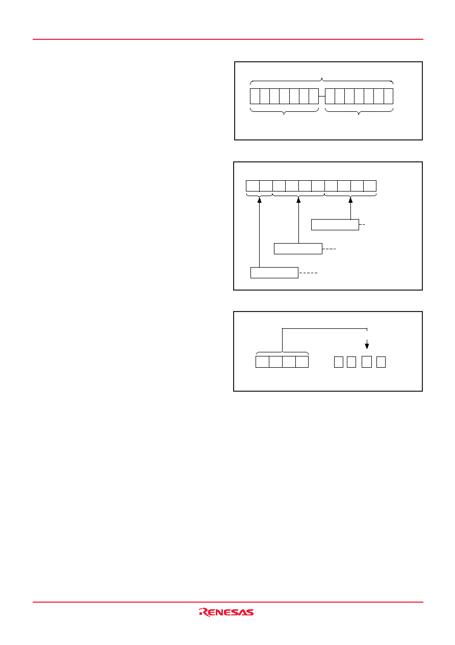
(8) Program counter (PC)
Program counter (PC) is used to specify a ROM address (page and
address). It determines a sequence in which instructions stored in
ROM are read. It is a binary counter that increments the number of
instruction bytes each time an instruction is executed. However,
the value changes to a specified address when branch instructions,
subroutine call instructions, return instructions, or the table refer-
ence instruction (TABP p) is executed.
Program counter consists of PCH (most significant bit to bit 7)
which specifies to a ROM page and PCL (bits 6 to 0) which speci-
fies an address within a page. After it reaches the last address
(address 127) of a page, it specifies address 0 of the next page
(Figure 7).
Make sure that the PCH does not specify after the last page of the
built-in ROM.
(9) Data pointer (DP)
Data pointer (DP) is used to specify a RAM address and consists
of registers Z, X, and Y. Register Z specifies a RAM file group, reg-
ister X specifies a file, and register Y specifies a RAM digit (Figure
8).
Register Y is also used to specify the port D bit position.
When using port D, set the port D bit position to register Y certainly
and execute the SD, RD, or SZD instruction (Figure 9).
Note
Register Z of data pointer is undefined after system is released
from reset.
Also, registers Z, X and Y are undefined in the RAM back-up. After
system is returned from the RAM back-up, set these registers.
Fig. 7 Program counter (PC) structure
Fig. 8 Data pointer (DP) structure
Fig. 9 SD instruction execution example
p5 p4 p3 p2 p1 p0
a6 a5 a4 a3 a2 a1 a0
Program counter
PCH
Specifying page
PCL
Specifying address
p6
Z1 Z0 X3 X2 X1 X0 Y3 Y2 Y1 Y0
Data pointer (DP)
Register Z (2)
Register X (4)
Register Y (4)
Specifying
RAM digit
Specifying RAM file
Specifying RAM file group
0
01
1
Set
Specifying bit position
Port D output latch
Register Y (4)
D2
D3
D1
D0
0
相关PDF资料 |
PDF描述 |
|---|---|
| M34509G4FP | 4-BIT, OTPROM, 6 MHz, MICROCONTROLLER, PDSO24 |
| M34509G4HFP | 4-BIT, OTPROM, 6 MHz, MICROCONTROLLER, PDSO24 |
| M34509G4-XXXFP | 4-BIT, OTPROM, 6 MHz, MICROCONTROLLER, PDSO24 |
| M34509G4H-XXXFP | 4-BIT, OTPROM, 6 MHz, MICROCONTROLLER, PDSO24 |
| M34510M4A-XXXSP | 4-BIT, MROM, 6 MHz, MICROCONTROLLER, PDIP32 |
相关代理商/技术参数 |
参数描述 |
|---|---|
| M34509G4FP | 制造商:RENESAS 制造商全称:Renesas Technology Corp 功能描述:SINGLE-CHIP 4-BIT CMOS MICROCOMPUTER |
| M34509G4HFP | 制造商:RENESAS 制造商全称:Renesas Technology Corp 功能描述:SINGLE-CHIP 4-BIT CMOS MICROCOMPUTER |
| M34509G4H-XXXFP | 制造商:RENESAS 制造商全称:Renesas Technology Corp 功能描述:SINGLE-CHIP 4-BIT CMOS MICROCOMPUTER |
| M34509G4-XXXFP | 制造商:RENESAS 制造商全称:Renesas Technology Corp 功能描述:SINGLE-CHIP 4-BIT CMOS MICROCOMPUTER |
| M34509T2-CPE | 功能描述:DEV TOOL COMPACT EMULATOR: 4508/ RoHS:否 类别:编程器,开发系统 >> 内电路编程器、仿真器以及调试器 系列:- 产品变化通告:Development Systems Discontinuation 19/Jul/2010 标准包装:1 系列:* 类型:* 适用于相关产品:* 所含物品:* |
发布紧急采购,3分钟左右您将得到回复。