- 您现在的位置:买卖IC网 > PDF目录69011 > M34513E4SP 4-BIT, OTPROM, 4.2 MHz, MICROCONTROLLER, PDIP32 PDF资料下载
参数资料
| 型号: | M34513E4SP |
| 元件分类: | 微控制器/微处理器 |
| 英文描述: | 4-BIT, OTPROM, 4.2 MHz, MICROCONTROLLER, PDIP32 |
| 封装: | 0.400 INCH, 1.78 MM PITCH, PLASTIC, SDIP-32 |
| 文件页数: | 30/97页 |
| 文件大小: | 1276K |
| 代理商: | M34513E4SP |
第1页第2页第3页第4页第5页第6页第7页第8页第9页第10页第11页第12页第13页第14页第15页第16页第17页第18页第19页第20页第21页第22页第23页第24页第25页第26页第27页第28页第29页当前第30页第31页第32页第33页第34页第35页第36页第37页第38页第39页第40页第41页第42页第43页第44页第45页第46页第47页第48页第49页第50页第51页第52页第53页第54页第55页第56页第57页第58页第59页第60页第61页第62页第63页第64页第65页第66页第67页第68页第69页第70页第71页第72页第73页第74页第75页第76页第77页第78页第79页第80页第81页第82页第83页第84页第85页第86页第87页第88页第89页第90页第91页第92页第93页第94页第95页第96页第97页
35
4513/4514 Group
SINGLE-CHIP 4-BIT CMOS MICROCOMPUTER
MITSUBISHI MICROCOMPUTERS
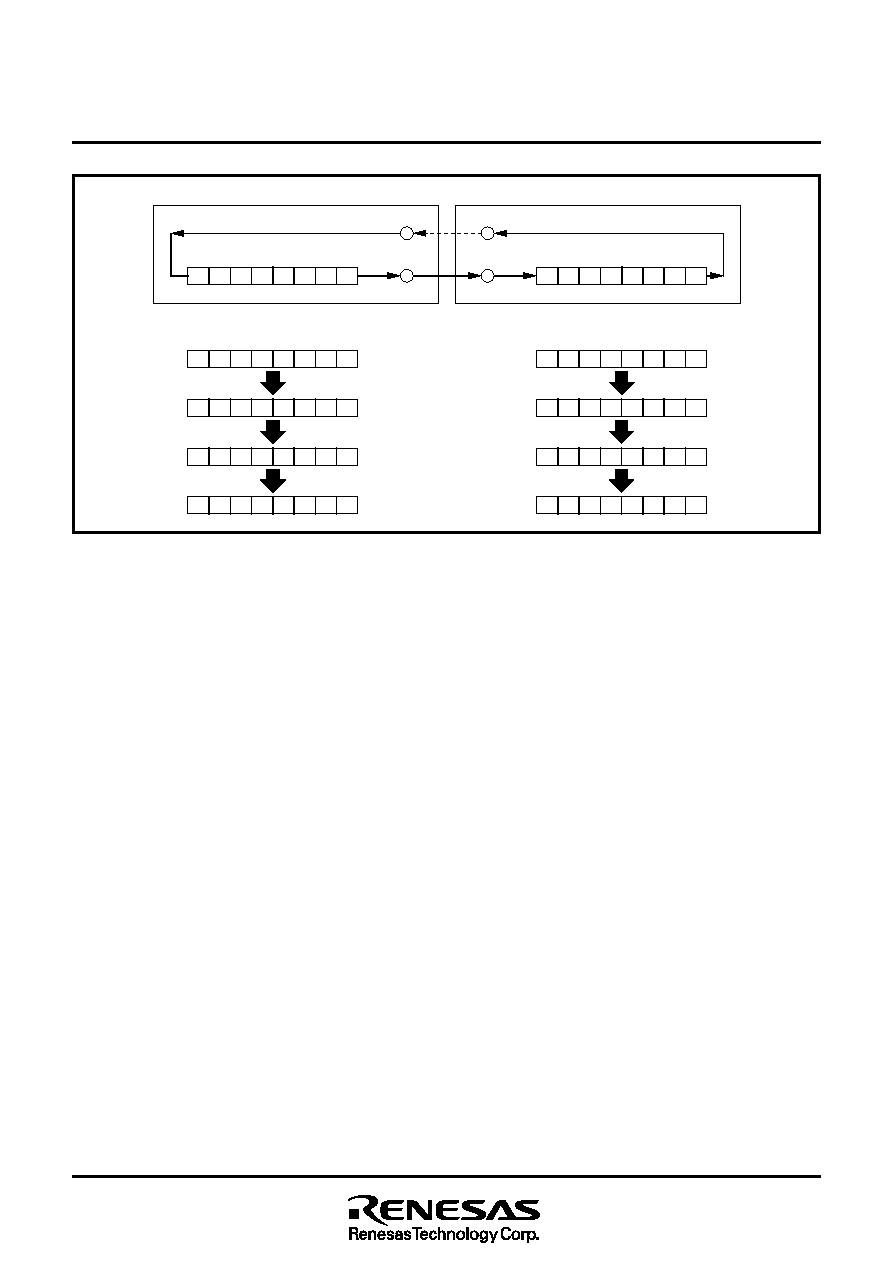
Fig. 23 Serial I/O register state when transferring
(1) Serial I/O register SI
Serial I/O register SI is the 8-bit data transfer serial/parallel conver-
sion register. Data can be set to register SI through registers A and
B with the TSIAB instruction. The contents of register A is transmit-
ted to the low-order 4 bits of register SI, and the contents of
register B is transmitted to the high-order 4 bits of register SI.
During transmission, each bit data is transmitted LSB first from the
lowermost bit (bit 0) of register SI, and during reception, each bit
data is received LSB first to register SI starting from the topmost bit
(bit 7).
When register SI is used as a work register without using serial I/O,
pull up the SCK pin or set the pin function to an input port P20.
(2) Serial I/O transmission/reception
completion flag (SIOF)
Serial I/O transmission/reception completion flag (SIOF) is set to
“1” when serial data transmission or reception completes. The
state of SIOF flag can be examined with the skip instruction
(SNZSI). Use the interrupt control register V2 to select the inter-
rupt or the skip instruction.
The SIOF flag is cleared to “0” when the interrupt occurs or when
the next instruction is skipped with the skip instruction.
When transmitting (D7–D0 : transfer data)
When receiving
D7 D6 D5 D4 D3 D2 D1 D0
SIN pin
SOUT pin
SOUT pin
SIN pin
Serial I/O register (SI)
D7 D6 D5 D4 D3 D2 D1 D0
D1 D0
Transfer data to be set
Transfer started
Transfer completed
D0
D7 D6 D5 D4 D3 D2
D7 D6 D5 D4 D3 D2 D1
D7 D6 D5 D4 D3 D2 D1 D0
(3) Serial I/O start instruction (SST)
When the SST instruction is executed, the SIOF flag is cleared to
“0” and then serial I/O transmission/reception is started.
(4) Serial I/O mode register J1
Register J1 controls the synchronous clock, P20/SCK, P21/SOUT
and P22/SIN pin function. Set the contents of this register through
register A with the TJ1A instruction. The TAJ1 instruction can be
used to transfer the contents of register J1 to register A.
相关PDF资料 |
PDF描述 |
|---|---|
| M34514M6-XXXFP | 4-BIT, MROM, 4.2 MHz, MICROCONTROLLER, PDSO42 |
| M34514E8FP | 4-BIT, OTPROM, 4.2 MHz, MICROCONTROLLER, PDSO42 |
| M34513M8-XXXFP | 4-BIT, MROM, 4.2 MHz, MICROCONTROLLER, PQFP32 |
| M34513M4-XXXSP | 4-BIT, MROM, 4.2 MHz, MICROCONTROLLER, PDIP32 |
| M34513M2-XXXFP | 4-BIT, MROM, 4.2 MHz, MICROCONTROLLER, PQFP32 |
相关代理商/技术参数 |
参数描述 |
|---|---|
| M34513E8 | 制造商:MITSUBISHI 制造商全称:Mitsubishi Electric Semiconductor 功能描述:SINGLE-CHIP 4-BIT CMOS MICROCOMPUTER |
| M34513E8FP | 制造商:RENESAS 制造商全称:Renesas Technology Corp 功能描述:SINGLE-CHIP 4-BIT CMOS MICROCOMPUTER |
| M34513M2 | 制造商:MITSUBISHI 制造商全称:Mitsubishi Electric Semiconductor 功能描述:SINGLE-CHIP 4-BIT CMOS MICROCOMPUTER |
| M34513M2-420FP | 制造商:MITSUBISHI 制造商全称:Mitsubishi Electric Semiconductor 功能描述:SINGLE-CHIP 4-BIT CMOS MICROCOMPUTER |
| M34513M2-XXXFP | 制造商:RENESAS 制造商全称:Renesas Technology Corp 功能描述:SINGLE-CHIP 4-BIT CMOS MICROCOMPUTER |
发布紧急采购,3分钟左右您将得到回复。