- 您现在的位置:买卖IC网 > PDF目录67762 > M37225ECSP 8-BIT, OTPROM, 8.1 MHz, MICROCONTROLLER, PDIP42 PDF资料下载
参数资料
| 型号: | M37225ECSP |
| 元件分类: | 微控制器/微处理器 |
| 英文描述: | 8-BIT, OTPROM, 8.1 MHz, MICROCONTROLLER, PDIP42 |
| 封装: | 0.600 INCH, 1.78 MM PITCH, PLASTIC, SDIP-42 |
| 文件页数: | 106/127页 |
| 文件大小: | 1897K |
| 代理商: | M37225ECSP |
第1页第2页第3页第4页第5页第6页第7页第8页第9页第10页第11页第12页第13页第14页第15页第16页第17页第18页第19页第20页第21页第22页第23页第24页第25页第26页第27页第28页第29页第30页第31页第32页第33页第34页第35页第36页第37页第38页第39页第40页第41页第42页第43页第44页第45页第46页第47页第48页第49页第50页第51页第52页第53页第54页第55页第56页第57页第58页第59页第60页第61页第62页第63页第64页第65页第66页第67页第68页第69页第70页第71页第72页第73页第74页第75页第76页第77页第78页第79页第80页第81页第82页第83页第84页第85页第86页第87页第88页第89页第90页第91页第92页第93页第94页第95页第96页第97页第98页第99页第100页第101页第102页第103页第104页第105页当前第106页第107页第108页第109页第110页第111页第112页第113页第114页第115页第116页第117页第118页第119页第120页第121页第122页第123页第124页第125页第126页第127页
7
SINGLE-CHIP 8-BIT CMOS MICROCOMPUTER for VOLTAGE SYNTHESIZER
with ON-SCREEN DISPLAY CONTROLLER
M37225M6/M8/MA/MC–XXXSP
M37225ECSP
MITSUBISHI MICROCOMPUTERS
Rev. 1.0
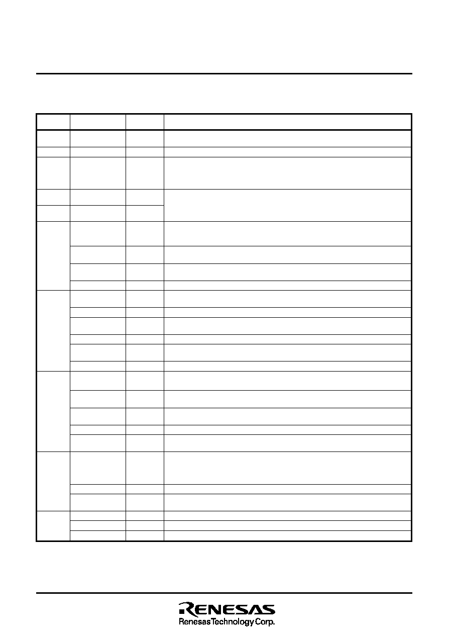
Pin
Name
Input/
Functions
Output
VCC,
Power source
Apply voltage of 5 V ± 10 % to (typical) VCC, and 0 V to VSS.
VSS
CNVSS
This is connected to VSS.
______
RESET
Reset input
Input
To enter the reset state, the reset input pin must be kept at a LOW for 2
s or more (under
normal VCC conditions).
If more time is needed for the quartz-crystal oscillator to stabilize, this LOW condition should
be maintained for the required time.
XIN
Clock input
Input
This chip has an internal clock generating circuit. To control generating frequency, an
external ceramic resonator or a quartz-crystal oscillator is connected between pins XIN and
XOUT
Clock output
Output
XOUT. If an external clock is used, the clock source should be connected to the XIN pin and
the XOUT pin should be left open.
P00/PWM0–
I/O port P0
I/O
Port P0 is an 8-bit I/O port with direction register allowing each I/O bit to be individually
P05/PWM5,
programmed as input or output. At reset, this port is set to input mode. The output structure
P06/INT2/A-D4,
is N-channel open-drain output. (See note 1)
P07/INT1
PWM output
Output
Pins P00–P05 are also used as PWM output pins PWM0–PWM5 respectively. The output
structure is N-channel open-drain output.
External interrupt
Input
Pins P06 and P07 are also used as INT external interrupt input pins INT2 and INT1
input
respectively.
Analog input
Input
P06 pin is also used as analog input pin A-D4.
P10/OUT2/A-D8, I/O port P1
I/O
Port P1 is an 8-bit I/O port and has basically the same functions as port P0. The
P11/SCL1,
output structure is CMOS output. (See note 1)
P12/SCL2,
OSD output
Output
Pins P10 is also used as OSD output pin OUT2. The output structure is CMOS output.
P13/SDA1,
Multi-master
I/O
Pins P11–P14 are used as SCL1, SCL2, SDA1 and SDA2 respectively, when multi-master
P14/SDA2,
I2C-BUS interface
I2C-BUS interface is used. The output structure is N-channel open-drain output.
P15/INT3/A-D1, Analog input
Input
Pins P10, P15–P17 are also used as analog input pin A-D8, A-D1–A-D3 respectively.
P16/A-D2,
External interrupt
Input
P15 pin is also used as INT external interrupt input pin INT3.
P17/DA2/A-D3
input
DA output
Output
Pins P17 is also used as 14-bit PWM output pin DA2. The output structure is CMOS output.
P20/SCLK,
I/O port P2
I/O
Port P2 is an 8-bit I/O port and has basically the same functions as port P0.
The P21/SOUT(/SIN), output structure is CMOS output. (See note 1)
P22/SIN,
Serial I/O synchronous
I/O
P20 pin is also used as serial I/O synchronous clock input/output pin SCLK. The output
P23/TIM3,
clock input/output port
structure is N-channel open-drain output.
P24/TIM2,
Serial I/O data
I/O
P21 pin is also used as serial I/O data input/output pin SOUT (/SIN). The output
P25–P27
input/output
structure is N-channel open-drain output.
Serial I/O data input
Input
P22 pin is also used as serial I/O data input pin SIN.
External clock
Input
Pins P23 and P24 are also used as timer external clock input pins TIM3 and TIM2
input for timer
respectively.
P30/A-D5,
I/O port P3
I/O
Ports P30–P32 and P35 are a 3-bit I/O port and has basically the same functions as port 0
P31/A-D6,
(see note 1). Either CMOS output or N-channel open-drain output structure can be selected
P32/A-D7,
as ports P30, P31 and P35. The output structure of port P3 2 is N-channel
DA1/P35
open-drain output structure.(See notes 1, 2)
Analog input
Input
Pins P30–P32 are also used as analog input pins A-D5–A-D7 respectively.
DA output
Output
P35 pin is also used as 14-bit PWM output pin DA1. The output structure is CMOS output. At
reset, output is undefined.
OSC1/P33, Input port P3
Input
Pins P33 and P34 are a 2-bit input port.
OSC2/P34, Clock input for OSD
Input
P33 pin is also used as OSD clock input pin OSC1.
Clock output for OSD
Output
P34 pin is also used as OSD clock output pin OSC2. The output structure is CMOS output.
7. PIN DESCRIPTION
Table 7.1 Pin Description
相关PDF资料 |
PDF描述 |
|---|---|
| M37270EF-XXXSP | 8-BIT, OTPROM, 8.1 MHz, MICROCONTROLLER, PDIP64 |
| M37270EFSP | 8-BIT, OTPROM, 8.1 MHz, MICROCONTROLLER, PDIP64 |
| M37270MF-XXXSP | 8-BIT, MROM, 8.1 MHz, MICROCONTROLLER, PDIP64 |
| M37271MF-XXXSP | 8-BIT, MROM, 8.1 MHz, MICROCONTROLLER, PDIP52 |
| M37271EF-XXXSP | 8-BIT, MROM, 8.1 MHz, MICROCONTROLLER, PDIP52 |
相关代理商/技术参数 |
参数描述 |
|---|---|
| M37225M6 | 制造商:RENESAS 制造商全称:Renesas Technology Corp 功能描述:SNGLE-CHIP 8-BIT CMOS MICROCOMPUTER for VOLTAGE SYNTHESIZER with ON-SCREEN DISPLAY CONTROLLER |
| M37225M8 | 制造商:RENESAS 制造商全称:Renesas Technology Corp 功能描述:SNGLE-CHIP 8-BIT CMOS MICROCOMPUTER for VOLTAGE SYNTHESIZER with ON-SCREEN DISPLAY CONTROLLER |
| M37225MA | 制造商:RENESAS 制造商全称:Renesas Technology Corp 功能描述:SNGLE-CHIP 8-BIT CMOS MICROCOMPUTER for VOLTAGE SYNTHESIZER with ON-SCREEN DISPLAY CONTROLLER |
| M372429100 | 制造商:ITW Switches 功能描述:IN-RUSH |
| M372429200 | 制造商:ITW Switches 功能描述:IN-RUSH |
发布紧急采购,3分钟左右您将得到回复。