- 您现在的位置:买卖IC网 > PDF目录80512 > M37540E8GP 8-BIT, OTPROM, 6 MHz, MICROCONTROLLER, PDSO36 PDF资料下载
参数资料
| 型号: | M37540E8GP |
| 元件分类: | 微控制器/微处理器 |
| 英文描述: | 8-BIT, OTPROM, 6 MHz, MICROCONTROLLER, PDSO36 |
| 封装: | 0.450 INCH, 0.80 MM PITCH, PLASTIC, SSOP-36 |
| 文件页数: | 31/90页 |
| 文件大小: | 830K |
| 代理商: | M37540E8GP |
第1页第2页第3页第4页第5页第6页第7页第8页第9页第10页第11页第12页第13页第14页第15页第16页第17页第18页第19页第20页第21页第22页第23页第24页第25页第26页第27页第28页第29页第30页当前第31页第32页第33页第34页第35页第36页第37页第38页第39页第40页第41页第42页第43页第44页第45页第46页第47页第48页第49页第50页第51页第52页第53页第54页第55页第56页第57页第58页第59页第60页第61页第62页第63页第64页第65页第66页第67页第68页第69页第70页第71页第72页第73页第74页第75页第76页第77页第78页第79页第80页第81页第82页第83页第84页第85页第86页第87页第88页第89页第90页
7540 Group
Rev.4.00
Jun 21, 2004
page 35 of 82
REJ03B0011-0400Z
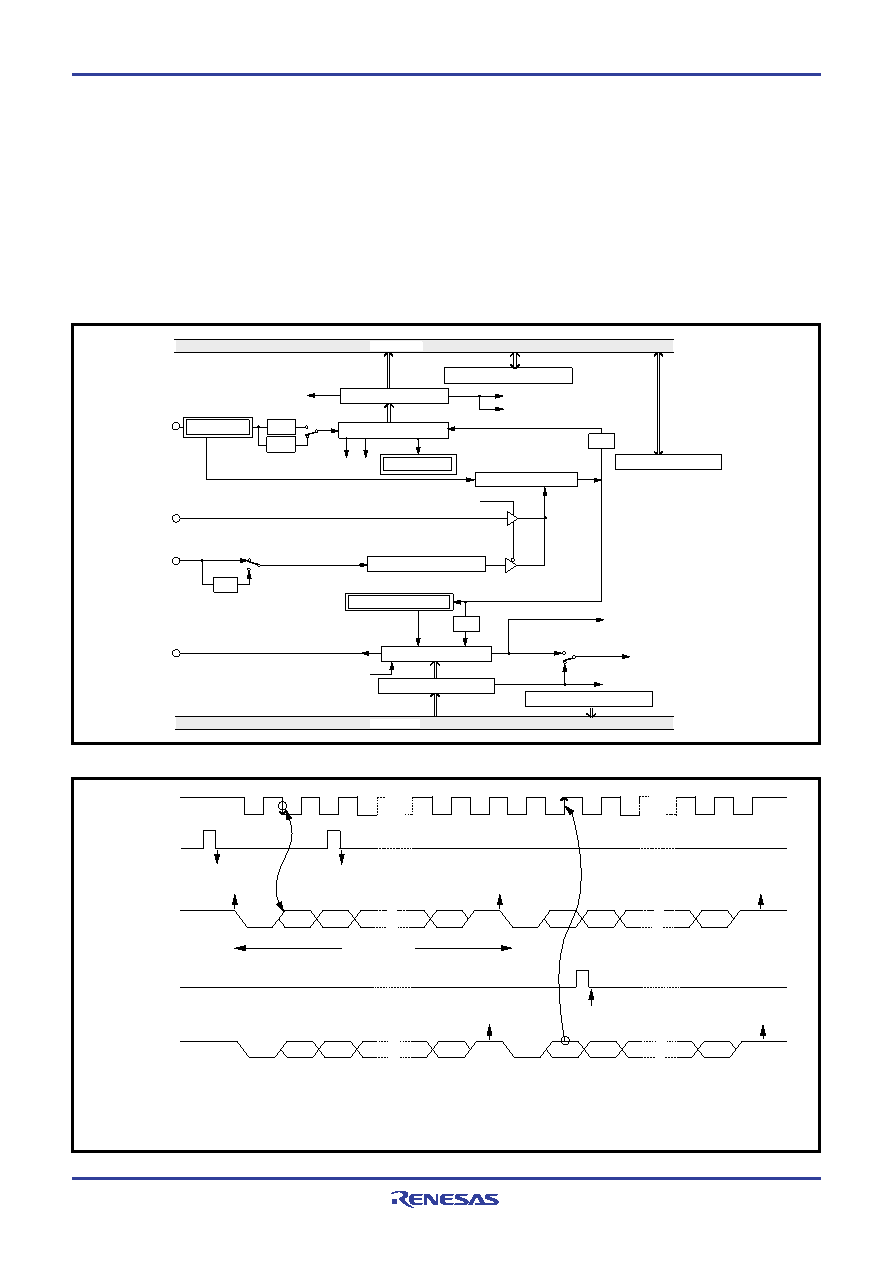
Fig. 32 Block diagram of UART serial I/O1
(2) Asynchronous Serial I/O (UART) Mode
Clock asynchronous serial I/O mode (UART) can be selected by
clearing the serial I/O1 mode selection bit of the serial I/O1 control
register to “0”.
Eight serial data transfer formats can be selected, and the transfer
formats used by a transmitter and receiver must be identical.
XIN
1/4
OE
PE FE
1/16
Data bus
Receive buffer register
Address 001816
Receive shift register
Receive buffer full flag (RBF)
Receive interrupt request (RI)
Baud rate generator
Frequency division ratio 1/(n+1)
Address 001C16
ST/SP/PA generator
Transmit buffer register
Data bus
Transmit shift register
Address 001816
Transmit shift completion flag (TSC)
Transmit buffer empty flag (TBE)
Transmit interrupt request (TI)
Address 001916
ST detector
SP detector
UART control register
Address 001B16
Character length selection bit
Address 001A16
BRG count source selection bit
Transmit interrupt source selection bit
Serial I/O1 synchronous clock selection bit
Clock control circuit
Character length selection bit
7 bits
8 bits
Serial I/O1 control register
P12/SCLK1
Serial I/O1 status register
P10/RXD1
P11/TXD1
The transmit and receive shift registers each have a buffer, but the
two buffers have the same address in memory. Since the shift reg-
ister cannot be written to or read from directly, transmit data is
written to the transmit buffer register, and receive data is read
from the receive buffer register.
The transmit buffer register can also hold the next data to be
transmitted, and the receive buffer register can hold a character
while the next character is being received.
Fig. 33 Operation of UART serial I/O1 function
TSC=0
TBE=1
RBF=0
TBE=0
RBF=1
ST
D0
D1
SP
D0
D1
ST
SP
TBE=1
TSC=1
ST
D0
D1
SP
D0
D1
ST
SP
Transmit or receive clock
Transmit buffer write
signal
Generated at 2nd bit in 2-stop-bit mode
1 start bit
7 or 8 data bit
1 or 0 parity bit
1 or 2 stop bit (s)
1: Error flag detection occurs at the same time that the RBF flag becomes “1” (at 1st stop bit, during reception).
2: As the transmit interrupt (TI), when either the TBE or TSC flag becomes “1,” can be selected to occur depending on the setting of the transmit
interrupt source selection bit (TIC) of the serial I/O1 control register.
3: The receive interrupt (RI) is set when the RBF flag becomes “1.”
4: After data is written to the transmit buffer when TSC=1, 0.5 to 1.5 cycles of the data shift cycle is necessary until changing to TSC=0.
Notes
Serial output TXD
Serial input RXD
Receive buffer read
signal
相关PDF资料 |
PDF描述 |
|---|---|
| M38224M6MXXXFP | 8-BIT, MROM, 4 MHz, MICROCONTROLLER, PQFP80 |
| M38227MCA-XXXFP | 8-BIT, MROM, 5 MHz, MICROCONTROLLER, PQFP80 |
| MB96F348AWAXXXPMC-GSE2 | 16-BIT, FLASH, 56 MHz, RISC MICROCONTROLLER, PQFP100 |
| MB90348CESPFV | MICROCONTROLLER, PQFP100 |
| MB90F346CESPFV | MICROCONTROLLER, PQFP100 |
相关代理商/技术参数 |
参数描述 |
|---|---|
| M37540E8GP#U0 | 功能描述:IC 7540 MCU OTP 32K 32LQFP RoHS:是 类别:集成电路 (IC) >> 嵌入式 - 微控制器, 系列:740/38000 产品培训模块:CAN Basics Part-1 CAN Basics Part-2 Electromagnetic Noise Reduction Techniques Part 1 M16C Product Overview Part 1 M16C Product Overview Part 2 标准包装:1 系列:M16C™ M32C/80/87 核心处理器:M32C/80 芯体尺寸:16/32-位 速度:32MHz 连通性:EBI/EMI,I²C,IEBus,IrDA,SIO,UART/USART 外围设备:DMA,POR,PWM,WDT 输入/输出数:121 程序存储器容量:384KB(384K x 8) 程序存储器类型:闪存 EEPROM 大小:- RAM 容量:24K x 8 电压 - 电源 (Vcc/Vdd):3 V ~ 5.5 V 数据转换器:A/D 34x10b,D/A 2x8b 振荡器型:内部 工作温度:-20°C ~ 85°C 封装/外壳:144-LQFP 包装:托盘 产品目录页面:749 (CN2011-ZH PDF) 配用:R0K330879S001BE-ND - KIT DEV RSK M32C/87 |
| M37540E8SP | 制造商:Renesas Electronics Corporation 功能描述: |
| M37540E8T-XXXFP | 制造商:RENESAS 制造商全称:Renesas Technology Corp 功能描述:SINGLE-CHIP 8-BIT CMOS MICROCOMPUTER |
| M37540E8T-XXXGP | 制造商:RENESAS 制造商全称:Renesas Technology Corp 功能描述:8-BIT CISC SINGLE-CHIP MICROCOMPUTER 740 FAMILY / 740 SERIES |
| M37540E8V-XXXFP | 制造商:RENESAS 制造商全称:Renesas Technology Corp 功能描述:SINGLE-CHIP 8-BIT CMOS MICROCOMPUTER |
发布紧急采购,3分钟左右您将得到回复。