- 您现在的位置:买卖IC网 > PDF目录80361 > M37547G4FP 8-BIT, MROM, 8 MHz, MICROCONTROLLER, PDSO36 PDF资料下载
参数资料
| 型号: | M37547G4FP |
| 元件分类: | 微控制器/微处理器 |
| 英文描述: | 8-BIT, MROM, 8 MHz, MICROCONTROLLER, PDSO36 |
| 封装: | 8.40 X 15 MM, 0.80 MM PITCH, PLASTIC, SSOP-36 |
| 文件页数: | 7/99页 |
| 文件大小: | 1029K |
| 代理商: | M37547G4FP |
第1页第2页第3页第4页第5页第6页当前第7页第8页第9页第10页第11页第12页第13页第14页第15页第16页第17页第18页第19页第20页第21页第22页第23页第24页第25页第26页第27页第28页第29页第30页第31页第32页第33页第34页第35页第36页第37页第38页第39页第40页第41页第42页第43页第44页第45页第46页第47页第48页第49页第50页第51页第52页第53页第54页第55页第56页第57页第58页第59页第60页第61页第62页第63页第64页第65页第66页第67页第68页第69页第70页第71页第72页第73页第74页第75页第76页第77页第78页第79页第80页第81页第82页第83页第84页第85页第86页第87页第88页第89页第90页第91页第92页第93页第94页第95页第96页第97页第98页第99页
REJ03B0156-0122
Rev.1.22
Mar 31, 2009
page 13 of 94
7547 Group
I/O Ports
[Direction registers] PiD
The I/O ports have direction registers which determine the input/
output direction of each pin. Each bit in a direction register corre-
sponds to one pin, and each pin can be set to be input or output.
When “1” is set to the bit corresponding to a pin, this pin becomes
an output port. When “0” is set to the bit, the pin becomes an in-
put port.
When data is read from a pin set to output, not the value of the pin
itself but the value of port latch is read. Pins set to input are float-
ing, and permit reading pin values.
If a pin set to input is written to, only the port latch is written to and
the pin remains floating.
[Port P0P3 drive capacity control register] DCCR
By setting the Port P0P3 drive capacity control register (address
001516), the drive capacity of the N-channel output transistor for
the port P0 and port P3 can be selected.
[Pull-up control register] PULL
By setting the pull-up control register (address 001616), ports P0
and P3 can exert pull-up control by program. However, pins set to
output are disconnected from this control and cannot exert pull-up
control.
[Port P1P3 control register] P1P3C
By setting the port P1P3 control register (address 001716), a
CMOS input level or a TTL input level can be selected for ports
P10, P12, P13, P36, and P37 by program.
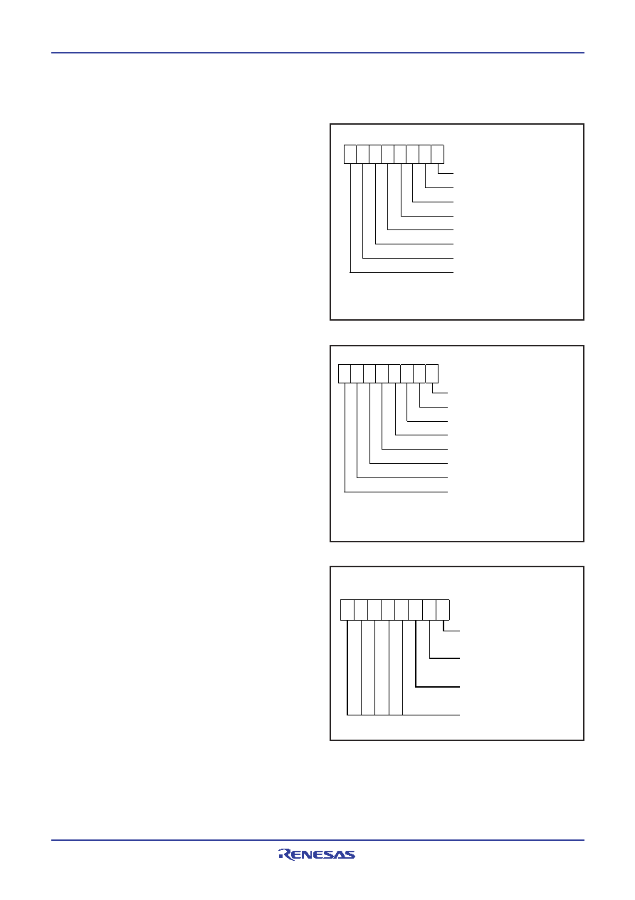
Fig. 12 Structure of port P1P3 control register
Fig. 11 Structure of pull-up control register
Port P1P3 control register
(P1P3C: address 001716, initial value: 0016)
b7
b0
Not used
1 : TTL level
0 : CMOS level
P10,P12,P13 input level selection bit
1 : TTL level
0 : CMOS level
P36/INT1 input level selection bit
1 : TTL level
0 : CMOS level
P37/INT0 input level selection bit
Pull-up control register
(PULL: address 001616, initial value: 0016)
P00 pull-up control bit
P01, P02 pull-up control bit
P03–P07 pull-up control bit
P30 pull-up control bit
P31, P32 pull-up control bit
P33 pull-up control bit
P34, P35 pull-up control bit
P36, P37 pull-up control bit
b7
b0
0 : Pull-up Off
1 : Pull-up On
Note : Pins set to output ports are disconnected from pull-up control.
Port P0P3 drive capacity control register
(DCCR: address 001516, initial value: 0016)
Port P00 drive capacity bit
Ports P01, P02 drive capacity bit
Ports P03–P07 drive capacity bit
Port P30 drive capacity bit
Ports P31, P32 drive capacity bit
Port P33 drive capacity bit
Ports P34, P35 drive capacity bit
Ports P36, P37 drive capacity bit
b7
b0
0 : Low
1 : High
Note: Number of LED drive port (drive capacity is HIGH) is 8-port.
Fig. 10 Structure of port P0P3 drive capacity control register
相关PDF资料 |
PDF描述 |
|---|---|
| M38047M8-XXXSP | 8-BIT, MROM, 8.4 MHz, MICROCONTROLLER, PDIP64 |
| M38234G4-XXXHP | 8-BIT, MROM, 10 MHz, MICROCONTROLLER, PQFP80 |
| M102P0200.0000DK | 200 MHz, OTHER CLOCK GENERATOR, MDIP24 |
| M30800SFP | 16-BIT, MROM, 20 MHz, MICROCONTROLLER, PQFP100 |
| M38C24M4-XXXFP | 8-BIT, MROM, 4 MHz, MICROCONTROLLER, PQFP64 |
相关代理商/技术参数 |
参数描述 |
|---|---|
| M37547G4FP#U0 | 功能描述:MCU 2/5V 16K 36-SSOP RoHS:是 类别:集成电路 (IC) >> 嵌入式 - 微控制器, 系列:740/38000 标准包装:250 系列:80C 核心处理器:8051 芯体尺寸:8-位 速度:16MHz 连通性:EBI/EMI,I²C,UART/USART 外围设备:POR,PWM,WDT 输入/输出数:40 程序存储器容量:- 程序存储器类型:ROMless EEPROM 大小:- RAM 容量:256 x 8 电压 - 电源 (Vcc/Vdd):4.5 V ~ 5.5 V 数据转换器:A/D 8x10b 振荡器型:内部 工作温度:-40°C ~ 85°C 封装/外壳:68-LCC(J 形引线) 包装:带卷 (TR) |
| M37547G4-XXXFP | 制造商:RENESAS 制造商全称:Renesas Technology Corp 功能描述:SINGLE-CHIP 8-BIT CMOS MICROCOMPUTER |
| M37548G1FP | 制造商:RENESAS 制造商全称:Renesas Technology Corp 功能描述:SINGLE-CHIP 8-BIT CMOS MICROCOMPUTER |
| M37548G1-XXXFP | 制造商:RENESAS 制造商全称:Renesas Technology Corp 功能描述:SINGLE-CHIP 8-BIT CMOS MICROCOMPUTER |
| M37548G2FP | 制造商:RENESAS 制造商全称:Renesas Technology Corp 功能描述:SINGLE-CHIP 8-BIT CMOS MICROCOMPUTER |
发布紧急采购,3分钟左右您将得到回复。