- 您现在的位置:买卖IC网 > PDF目录67763 > M37920F8CHP 16-BIT, FLASH, 20 MHz, MICROCONTROLLER, PQFP100 PDF资料下载
参数资料
| 型号: | M37920F8CHP |
| 元件分类: | 微控制器/微处理器 |
| 英文描述: | 16-BIT, FLASH, 20 MHz, MICROCONTROLLER, PQFP100 |
| 封装: | 14 X 14 MM, 0.50 MM PITCH, PLASTIC, LQFP-100 |
| 文件页数: | 10/155页 |
| 文件大小: | 1274K |
| 代理商: | M37920F8CHP |
第1页第2页第3页第4页第5页第6页第7页第8页第9页当前第10页第11页第12页第13页第14页第15页第16页第17页第18页第19页第20页第21页第22页第23页第24页第25页第26页第27页第28页第29页第30页第31页第32页第33页第34页第35页第36页第37页第38页第39页第40页第41页第42页第43页第44页第45页第46页第47页第48页第49页第50页第51页第52页第53页第54页第55页第56页第57页第58页第59页第60页第61页第62页第63页第64页第65页第66页第67页第68页第69页第70页第71页第72页第73页第74页第75页第76页第77页第78页第79页第80页第81页第82页第83页第84页第85页第86页第87页第88页第89页第90页第91页第92页第93页第94页第95页第96页第97页第98页第99页第100页第101页第102页第103页第104页第105页第106页第107页第108页第109页第110页第111页第112页第113页第114页第115页第116页第117页第118页第119页第120页第121页第122页第123页第124页第125页第126页第127页第128页第129页第130页第131页第132页第133页第134页第135页第136页第137页第138页第139页第140页第141页第142页第143页第144页第145页第146页第147页第148页第149页第150页第151页第152页第153页第154页第155页
107
M37920F8CGP, M37920F8CHP, M37920FCCGP
M37920FCCHP, M37920FGCGP, M37920FGCHP
PRELIMINAR
Y
Notice:
This
is not
a final
specification.
Some
parametric
limits
are
subject
to change.
SINGLE-CHIP 16-BIT CMOS MICROCOMPUTER FLASH MEMORY VERSION
MITSUBISHI MICROCOMPUTERS
POWER SAVING FUNCTION
The following functions can save the power dissipation of the whole
system.
(1) Bus fixation in STP and WIT modes
By setting the standby state select bit (bit 2 of the particular function
select register 1) to “1”, in the stop or wait state, the I/O pins of the
external buses and bus control signals can be switched to program-
mable I/O port pins. By setting these pins’ state with the correspond-
ing port registers and port direction registers, unnecessary current
will not flow between the microcomputer and external devices. As a
result, in the stop or wait mode, the power dissipation of the whole
system can be saved. Table 24 lists the correspondence between
the external buses, bus control signals, and programmable I/O port
pins.
This function is valid only in the stop or wait state. At termination of
the stop or wait mode, the original functions of external buses and
bus control signals become valid.
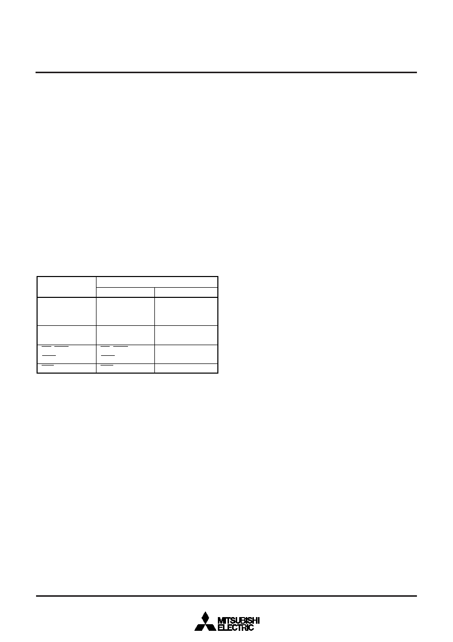
Table 24. Correspondence between external buses, bus control sig-
nals, and programmable I/O port pins
External buses,
Bus control signals
A0 to A7,
A8 to A15,
A16 to A23
0
Standby state select bit
A0 to A7,
A8 to A15,
A16 to A23
1
D0 to D7,
D8 to D15 (Note 1)
D0 to D7,
D8 to D15
P100 to P107 (Note 2),
P110 to P117 (Note 2),
P00 to P07 (Note 2)
P10 to P17 (Note 2),
P20 to P27
RD, BLW,
BHW
RD, BLW,
BHW (Note 1)
P31, P32 (Note 2),
P33
CS0
P90 (Note 2)
Notes 1: When the external data bus width = 8 bits (BYTE = VCC level),
this becomes a programmable I/O port pin, regardless of the
standby state select bit’s contents.
2: Pin functions of port pins P0, P1, P31, P32, P90, P10, P11 are
not shown in the pin configuration. However, relationship with
corresponding bus signals and ports is listed in Table 24. For
the addresses of these port’s registers and direction registers,
refer to the location of the perpheral devices’ control register
(Figures 4 and 5).
(2) Stop of internal clock in wait mode
In the WIT mode, if the internal peripheral devices need not to be
operated, be sure to set the internal clock stop select bit at WIT (bit 3
of the particular function select register 1) to “1”. As a result, the clock
source for each internal peripheral device is stopped, and the power
dissipation of the microcomputer can be saved.
For details, refer to the section on the Stop and Wait modes.
(3) Stop of oscillation circuit
When an externally-generated-stable clock is input to pin XIN, the
power dissipation can be saved if both of the following conditions are
met:
the external clock input select bit (bit 1 of the particular function
select register 0) = “1”.
the oscillation driver circuit between pins XIN and XOUT stops its
operation.
At this time, the output level at pin XOUT is fixed to “H”. When the STP
mode is terminated by an interrupt request occurrence, the watch-
dog timer is not used. Therefore, an instruction can be executed just
after the termination of the STP mode. For details, refer to the sec-
tion on the clock generating circuit and stop and wait modes.
(4) Disconnection from pin VREF
When not using the A-D converter, by setting the VREF connection
select bit (bit 6 of the A-D control register 1) to “1”, the ladder network
of the A-D converter will be disconnected from the reference voltage
input pin (VREF). In this case, no current flows from pin VREF to the
ladder network, and the power dissipation can be saved. Note that,
after the VREF connection select bit changes from “1” (VREF discon-
nected) to “0” (VREF connected), be sure that the A-D conversion
starts a period of 1 s or more has elapsed. For details, refer to the
section on the A-D converter.
相关PDF资料 |
PDF描述 |
|---|---|
| M37920F8CGP | 16-BIT, FLASH, 20 MHz, MICROCONTROLLER, PQFP100 |
| M38039MFL-XXXHP | 8-BIT, MROM, 16.8 MHz, MICROCONTROLLER, PQFP64 |
| M38039MFL-XXXSP | 8-BIT, MROM, 16.8 MHz, MICROCONTROLLER, PDIP64 |
| M38039MFL-XXXWG | 8-BIT, MROM, 16.8 MHz, MICROCONTROLLER, PBGA64 |
| M38039FFLHP | 8-BIT, FLASH, 16.8 MHz, MICROCONTROLLER, PQFP64 |
相关代理商/技术参数 |
参数描述 |
|---|---|
| M37920FCCGP | 制造商:MITSUBISHI 制造商全称:Mitsubishi Electric Semiconductor 功能描述:SINGLE-CHIP 16-BIT CMOS MICROCOMPUTER FLASH MEMORY VERSION |
| M37920FCCHP | 制造商:MITSUBISHI 制造商全称:Mitsubishi Electric Semiconductor 功能描述:SINGLE-CHIP 16-BIT CMOS MICROCOMPUTER FLASH MEMORY VERSION |
| M37920FGCGP | 制造商:MITSUBISHI 制造商全称:Mitsubishi Electric Semiconductor 功能描述:SINGLE-CHIP 16-BIT CMOS MICROCOMPUTER FLASH MEMORY VERSION |
| M37920FGCHP | 制造商:MITSUBISHI 制造商全称:Mitsubishi Electric Semiconductor 功能描述:SINGLE-CHIP 16-BIT CMOS MICROCOMPUTER FLASH MEMORY VERSION |
| M37920S4CGP | 制造商:MITSUBISHI 制造商全称:Mitsubishi Electric Semiconductor 功能描述:16 BIT CMOS MICROCOMPUTER |
发布紧急采购,3分钟左右您将得到回复。