- 您现在的位置:买卖IC网 > PDF目录80361 > M38234G4-XXXHP 8-BIT, MROM, 10 MHz, MICROCONTROLLER, PQFP80 PDF资料下载
参数资料
| 型号: | M38234G4-XXXHP |
| 元件分类: | 微控制器/微处理器 |
| 英文描述: | 8-BIT, MROM, 10 MHz, MICROCONTROLLER, PQFP80 |
| 封装: | 12 X 12 MM, 0.50 MM PITCH, PLASTIC, LQFP-80 |
| 文件页数: | 35/64页 |
| 文件大小: | 922K |
| 代理商: | M38234G4-XXXHP |
第1页第2页第3页第4页第5页第6页第7页第8页第9页第10页第11页第12页第13页第14页第15页第16页第17页第18页第19页第20页第21页第22页第23页第24页第25页第26页第27页第28页第29页第30页第31页第32页第33页第34页当前第35页第36页第37页第38页第39页第40页第41页第42页第43页第44页第45页第46页第47页第48页第49页第50页第51页第52页第53页第54页第55页第56页第57页第58页第59页第60页第61页第62页第63页第64页
Rev.2.02
Jun 19, 2007
page 38 of 73
REJ03B0146-0202
3823 Group
A/D CONVERTER
[AD Conversion Register (ADH, ADL)] 003516
The AD conversion register is a read-only register that contains
the result of an A/D conversion. When reading this register during
an A/D conversion, the previous conversion result is read.The
high-order 8 bits of a conversion result is stored in the AD conver-
sion high-order register (address 003516),and the low-order 2 bits
of the same result are stored in bit 7 and bit 6 of the AD conver-
sion low-order register (address 003616).
The bit 0 in the AD conversion low-order register is used as the
conversion mode selection bit. 8-bit A/D mode is selected by set-
ting this bit to “0” and 10-bit A/D mode is selected by setting it to
“1”.
[AD Control Register (ADCON)] 003416
The AD control register controls the A/D conversion process. Bits
0 to 2 of this register select specific analog input pins. Bit 3 signals
the completion of an A/D conversion. The value of this bit remains
at “0” during an A/D conversion, then changes to “1” when the
A/D conversion is completed. Writing “0” to this bit starts the A/D
conversion. Bit 4 is the VREF input switch bit which controls con-
nection of the resistor ladder and the reference voltage input pin
(VREF). The resistor ladder is always connected to VREF when bit
4 is set to "1". When bit 4 is set to “0”, the resistor ladder is cut off
from VREF except for A/D conversion performed. When bit 5,
which is the AD external trigger valid bit, is set to “1”, this bit en-
ables A/D conversion even by a falling edge of an ADT input. Set
the P57/ADT pin to input mode (set "0" to bit 7 of port P5 direction
register) when using an A/D external trigger.
[Comparison Voltage Generator]
The comparison voltage generator divides the voltage between
AVSS and VREF, and outputs the divided voltages.
[Channel Selector]
The channel selector selects one of the input ports P67/AN7–P60/
AN0, and inputs it to the comparator.
[Comparator and Control Circuit]
The comparator and control circuit compares an analog input volt-
age with the comparison voltage and stores the result in the AD
conversion register. When an A/D conversion is completed, the
control circuit sets the AD conversion completion bit and the AD
interrupt request bit to “1”.
The comparator is constructed linked to a capacitor. The conver-
sion accuracy may be low because the charge is lost if the
conversion speed is not enough. Accordingly, set f(XIN) to at least
500kHz during A/D conversion in the middle-or high-speed mode.
Also, do not execute the STP or WIT instruction during an A/D
conversion.
In the low-speed mode, since the A/D conversion is executed by
the built-in self-oscillation circuit, the minimum value of f(XIN) fre-
quency is not limited.
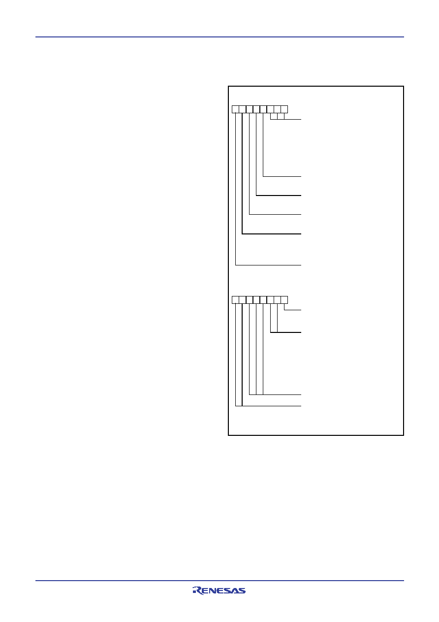
Fig. 33 Structure of AD conversion-related registers
AD control register
(ADCON : address 003416)
AD conversion completion bit
0 : Conversion in progress
1 : Conversion completed
Analog input pin selection bits
0 0 0 : P60/AN0
0 0 1 : P61/AN1
0 1 0 : P62/AN2
0 1 1 : P63/AN3
1 0 0 : P64/AN4
1 0 1 : P65/AN5
1 1 0 : P66/AN6
1 1 1 : P67/AN7
VREF input switch bit
0 : ON during conversion
1 : Always ON
AD external trigger valid bit
0 : A/D external trigger invalid
1 : A/D external trigger valid
b7
b0
Interrupt source selection bit
0 : Interrupt request at A/D
conversion completed
1 : Interrupt request at ADT
input falling
Not used (returns “0” when read)
AD conversion low-order register
(ADL : address 003616)
AD conversion speed selection bit
00 : f(XIN)/2
(this can be used in CPUM7 = “0” )
01 : f(XIN)
(this can be used in CPUM7 = “0” )
10 : On-chip oscillator
(this can be used in CPUM7 = “0”
and EXPCM0 = “1”)
11 : Disabled
Conversion mode selection bit
0 : 8 bit A/D mode
1 : 10 bit A/D mode
Not used (returns “0” when read)
In 10-bit A/D mode
A/D conversion data storage
In 8-bit A/D mode
Not used (Indefinite at read)
b7
b0
相关PDF资料 |
PDF描述 |
|---|---|
| M102P0200.0000DK | 200 MHz, OTHER CLOCK GENERATOR, MDIP24 |
| M30800SFP | 16-BIT, MROM, 20 MHz, MICROCONTROLLER, PQFP100 |
| M38C24M4-XXXFP | 8-BIT, MROM, 4 MHz, MICROCONTROLLER, PQFP64 |
| MAXQ610X-0000+ | 16-BIT, FLASH, 12 MHz, RISC MICROCONTROLLER, UUC |
| MB89P568-101PMC1 | 8-BIT, MROM, 12.5 MHz, MICROCONTROLLER, PQFP80 |
相关代理商/技术参数 |
参数描述 |
|---|---|
| M38235G6FP#U0 | 功能描述:MCU 2/5V 24K 80-QFP QZ-ROM RoHS:是 类别:集成电路 (IC) >> 嵌入式 - 微控制器, 系列:740/38000 标准包装:250 系列:80C 核心处理器:8051 芯体尺寸:8-位 速度:16MHz 连通性:EBI/EMI,I²C,UART/USART 外围设备:POR,PWM,WDT 输入/输出数:40 程序存储器容量:- 程序存储器类型:ROMless EEPROM 大小:- RAM 容量:256 x 8 电压 - 电源 (Vcc/Vdd):4.5 V ~ 5.5 V 数据转换器:A/D 8x10b 振荡器型:内部 工作温度:-40°C ~ 85°C 封装/外壳:68-LCC(J 形引线) 包装:带卷 (TR) |
| M38235G6HP#U0 | 功能描述:MCU 2/5V 24K 80-LQFP QZ-ROM RoHS:是 类别:集成电路 (IC) >> 嵌入式 - 微控制器, 系列:740/38000 标准包装:250 系列:80C 核心处理器:8051 芯体尺寸:8-位 速度:16MHz 连通性:EBI/EMI,I²C,UART/USART 外围设备:POR,PWM,WDT 输入/输出数:40 程序存储器容量:- 程序存储器类型:ROMless EEPROM 大小:- RAM 容量:256 x 8 电压 - 电源 (Vcc/Vdd):4.5 V ~ 5.5 V 数据转换器:A/D 8x10b 振荡器型:内部 工作温度:-40°C ~ 85°C 封装/外壳:68-LCC(J 形引线) 包装:带卷 (TR) |
| M38238G8FP#U0 | 功能描述:MCU 2/5V 32K 80-QFP QZ-ROM RoHS:是 类别:集成电路 (IC) >> 嵌入式 - 微控制器, 系列:740/38000 标准包装:250 系列:80C 核心处理器:8051 芯体尺寸:8-位 速度:16MHz 连通性:EBI/EMI,I²C,UART/USART 外围设备:POR,PWM,WDT 输入/输出数:40 程序存储器容量:- 程序存储器类型:ROMless EEPROM 大小:- RAM 容量:256 x 8 电压 - 电源 (Vcc/Vdd):4.5 V ~ 5.5 V 数据转换器:A/D 8x10b 振荡器型:内部 工作温度:-40°C ~ 85°C 封装/外壳:68-LCC(J 形引线) 包装:带卷 (TR) |
| M38238G8HP#U0 | 功能描述:MCU 2/5V 32K 80-LQFP QZ-ROM RoHS:是 类别:集成电路 (IC) >> 嵌入式 - 微控制器, 系列:740/38000 标准包装:250 系列:80C 核心处理器:8051 芯体尺寸:8-位 速度:16MHz 连通性:EBI/EMI,I²C,UART/USART 外围设备:POR,PWM,WDT 输入/输出数:40 程序存储器容量:- 程序存储器类型:ROMless EEPROM 大小:- RAM 容量:256 x 8 电压 - 电源 (Vcc/Vdd):4.5 V ~ 5.5 V 数据转换器:A/D 8x10b 振荡器型:内部 工作温度:-40°C ~ 85°C 封装/外壳:68-LCC(J 形引线) 包装:带卷 (TR) |
| M38239GCFP#U0 | 功能描述:MCU 2/5V 48K 80-QFP QZ-ROM RoHS:是 类别:集成电路 (IC) >> 嵌入式 - 微控制器, 系列:740/38000 标准包装:250 系列:80C 核心处理器:8051 芯体尺寸:8-位 速度:16MHz 连通性:EBI/EMI,I²C,UART/USART 外围设备:POR,PWM,WDT 输入/输出数:40 程序存储器容量:- 程序存储器类型:ROMless EEPROM 大小:- RAM 容量:256 x 8 电压 - 电源 (Vcc/Vdd):4.5 V ~ 5.5 V 数据转换器:A/D 8x10b 振荡器型:内部 工作温度:-40°C ~ 85°C 封装/外壳:68-LCC(J 形引线) 包装:带卷 (TR) |
发布紧急采购,3分钟左右您将得到回复。