- 您现在的位置:买卖IC网 > PDF目录80529 > M38869FFAHP 8-BIT, FLASH, 5 MHz, MICROCONTROLLER, PQFP80 PDF资料下载
参数资料
| 型号: | M38869FFAHP |
| 元件分类: | 微控制器/微处理器 |
| 英文描述: | 8-BIT, FLASH, 5 MHz, MICROCONTROLLER, PQFP80 |
| 封装: | 12 X 12 MM, 0.50 MM PITCH, PLASTIC, LQFP-80 |
| 文件页数: | 91/113页 |
| 文件大小: | 1871K |
| 代理商: | M38869FFAHP |
第1页第2页第3页第4页第5页第6页第7页第8页第9页第10页第11页第12页第13页第14页第15页第16页第17页第18页第19页第20页第21页第22页第23页第24页第25页第26页第27页第28页第29页第30页第31页第32页第33页第34页第35页第36页第37页第38页第39页第40页第41页第42页第43页第44页第45页第46页第47页第48页第49页第50页第51页第52页第53页第54页第55页第56页第57页第58页第59页第60页第61页第62页第63页第64页第65页第66页第67页第68页第69页第70页第71页第72页第73页第74页第75页第76页第77页第78页第79页第80页第81页第82页第83页第84页第85页第86页第87页第88页第89页第90页当前第91页第92页第93页第94页第95页第96页第97页第98页第99页第100页第101页第102页第103页第104页第105页第106页第107页第108页第109页第110页第111页第112页第113页
76
3886 Group
SINGLE-CHIP 8-BIT CMOS MICROCOMPUTER
MITSUBISHI MICROCOMPUTERS
Functional Outline (serial I/O mode)
In the serial I/O mode, data is transferred synchronously with the
clock using serial input/output. The input data is read from the
SDA pin into the internal circuit synchronously with the rising edge
of the serial clock pulse; the output data is output from the SDA
pin synchronously with the falling edge of the serial clock pulse.
Data is transferred in units of eight bits.
In the first transfer, the user inputs the command code. This is fol-
lowed by address input and data input/output according to the
contents of the command. Table 26 shows the software com-
mands used in the serial I/O mode. The following explains each
software command.
Table 26 Software command (serial I/O mode)
Read
Program
Program verify
Erase
Erase verify
Error check
Number of transfers
Command
First command
code input
0016
4016
C016
2016
A016
8016
Read address L (Input)
Program address L (Input)
Verify data (Output)
2016 (Input)
Verify address L (Input)
Error code (Output)
Second
Read address H (Input)
Program address H (Input)
—————
Verify address H (Input)
—————
Third
Fourth
Read data (Output)
Program data (Input)
—————
Verify data (Output)
—————
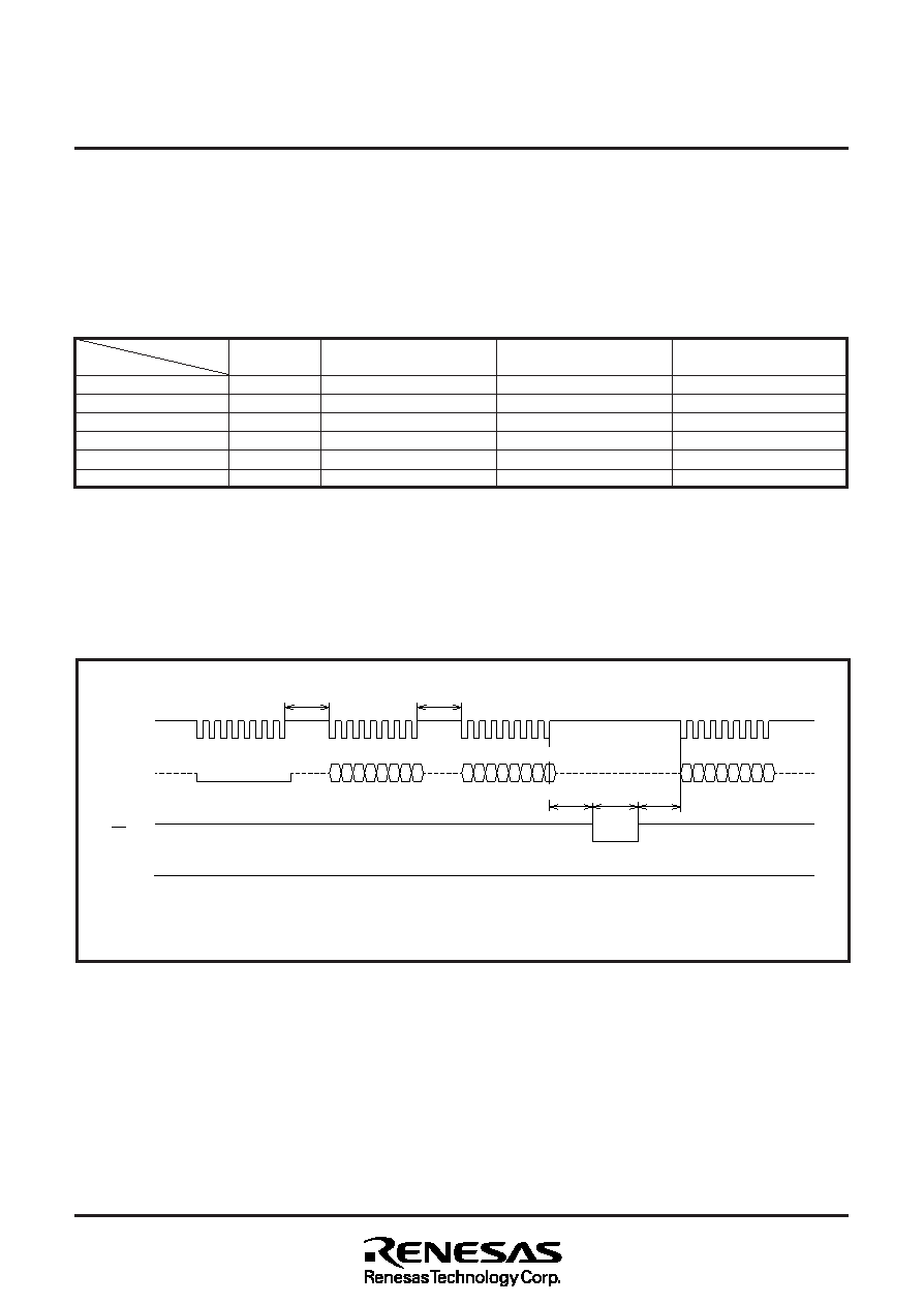
q Read command
Input command code 0016 in the first transfer. Proceed and input
the low-order 8 bits and the high-order 8 bits of the address and
__
pull the OE pin low. When this is done, the M38869FFAHP/GP
reads out the contents of the specified address, and then latchs it
__
into the internal data latch. When the OE pin is released back high
and serial clock is input to the SCLK pin, the read data that has
been latched into the data latch is serially output from the SDA
pin.
Fig. 73 Timings during reading
“L”
SCLK
BUSY
OE
SDA
tCH
A0
A7
A8
A15
D0
D7
tCH
tCR
Command code input (0016)
Read address input (L)
Read address input (H)
Read data output
tWR
Read
tRC
Note : When outputting the read data, the SDA pin is switched for output at the first falling edge of SCLK. The SDA pin is placed
in the floating state during the period of th(C-E) after the last rising edge of SCLK (at the 8th bit).
00000000
相关PDF资料 |
PDF描述 |
|---|---|
| MSP430F5419AIPZ | 16-BIT, FLASH, 25 MHz, RISC MICROCONTROLLER, PQFP100 |
| M30221M4-XXXFP | 16-BIT, MROM, 10 MHz, MICROCONTROLLER, PQFP120 |
| M38207M8-XXXHP | 8-BIT, MROM, 4 MHz, MICROCONTROLLER, PQFP80 |
| M38254M4DXXXFP | 8-BIT, MROM, 4 MHz, MICROCONTROLLER, PQFP100 |
| MB90341EPFV | MICROCONTROLLER, PQFP100 |
相关代理商/技术参数 |
参数描述 |
|---|---|
| M38869FFAHP#UU | 功能描述:IC 740/3886 MCU FLASH 80LQFP RoHS:是 类别:集成电路 (IC) >> 嵌入式 - 微控制器, 系列:740/38000 产品培训模块:CAN Basics Part-1 CAN Basics Part-2 Electromagnetic Noise Reduction Techniques Part 1 M16C Product Overview Part 1 M16C Product Overview Part 2 标准包装:1 系列:M16C™ M32C/80/87 核心处理器:M32C/80 芯体尺寸:16/32-位 速度:32MHz 连通性:EBI/EMI,I²C,IEBus,IrDA,SIO,UART/USART 外围设备:DMA,POR,PWM,WDT 输入/输出数:121 程序存储器容量:384KB(384K x 8) 程序存储器类型:闪存 EEPROM 大小:- RAM 容量:24K x 8 电压 - 电源 (Vcc/Vdd):3 V ~ 5.5 V 数据转换器:A/D 34x10b,D/A 2x8b 振荡器型:内部 工作温度:-20°C ~ 85°C 封装/外壳:144-LQFP 包装:托盘 产品目录页面:749 (CN2011-ZH PDF) 配用:R0K330879S001BE-ND - KIT DEV RSK M32C/87 |
| M38869FF-XXXHP | 制造商:RENESAS 制造商全称:Renesas Technology Corp 功能描述:SINGLE-CHIP 8-BIT CMOS MICROCOMPUTER |
| M38869M1-XXXHP | 制造商:RENESAS 制造商全称:Renesas Technology Corp 功能描述:SINGLE-CHIP 8-BIT CMOS MICROCOMPUTER |
| M38869M2-XXXHP | 制造商:RENESAS 制造商全称:Renesas Technology Corp 功能描述:SINGLE-CHIP 8-BIT CMOS MICROCOMPUTER |
| M38869M3-XXXHP | 制造商:RENESAS 制造商全称:Renesas Technology Corp 功能描述:SINGLE-CHIP 8-BIT CMOS MICROCOMPUTER |
发布紧急采购,3分钟左右您将得到回复。