- 您现在的位置:买卖IC网 > PDF目录80549 > M38D58G8-XXXHP 8-BIT, MROM, 6.25 MHz, MICROCONTROLLER, PQFP80 PDF资料下载
参数资料
| 型号: | M38D58G8-XXXHP |
| 元件分类: | 微控制器/微处理器 |
| 英文描述: | 8-BIT, MROM, 6.25 MHz, MICROCONTROLLER, PQFP80 |
| 封装: | 12 X 12 MM, 0.50 MM PITCH, PLASTIC, LQFP-80 |
| 文件页数: | 129/142页 |
| 文件大小: | 2004K |
| 代理商: | M38D58G8-XXXHP |
第1页第2页第3页第4页第5页第6页第7页第8页第9页第10页第11页第12页第13页第14页第15页第16页第17页第18页第19页第20页第21页第22页第23页第24页第25页第26页第27页第28页第29页第30页第31页第32页第33页第34页第35页第36页第37页第38页第39页第40页第41页第42页第43页第44页第45页第46页第47页第48页第49页第50页第51页第52页第53页第54页第55页第56页第57页第58页第59页第60页第61页第62页第63页第64页第65页第66页第67页第68页第69页第70页第71页第72页第73页第74页第75页第76页第77页第78页第79页第80页第81页第82页第83页第84页第85页第86页第87页第88页第89页第90页第91页第92页第93页第94页第95页第96页第97页第98页第99页第100页第101页第102页第103页第104页第105页第106页第107页第108页第109页第110页第111页第112页第113页第114页第115页第116页第117页第118页第119页第120页第121页第122页第123页第124页第125页第126页第127页第128页当前第129页第130页第131页第132页第133页第134页第135页第136页第137页第138页第139页第140页第141页第142页
Rev.3.04
May 20, 2008
REJ03B0158-0304
38D5 Group
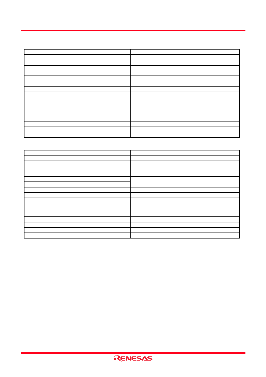
Table 20
Description of pin function (Flash Memory Standard Serial I/O Mode 1)
Pin name
Signal name
I/O
Function
VCC,VSS
Power supply
I
Apply 2.7 to 5.5 V to the VCC pin and 0 V to the Vss pin.
CNVSS
I
After input of port is set, input “H” level.
RESET
Reset input
I
Reset input pin. To reset the microcomputer, RESET pin should be
held at an “L” level for 16 cycles or more of XIN.
XIN
Clock input
I
Connect an oscillation circuit between the XIN and XOUT pins.
As for the connection method, refer to the “clock generating circuit”.
XOUT
Clock output
O
AVSS
Analog power supply input
Connect AVss to VSS.
VREF
Reference voltage input
I
Apply reference voltage of A/D convertor to this pin.
P00
P07, P10P17,
P20
P27, P30P37,
P40
P47, P50P57,
P60
P67, P72P74
I/O port
I/O
Input “L” or “H” level, or keep open.
P40
RxD input
I
Serial data input pin.
P41
TxD output
O
Serial data output pin.
P42
SCLK input
I
Serial clock input pin.
P43
BUSY output
O
BUSY signal output pin.
Table 21
Description of pin function (Flash Memory Standard Serial I/O Mode 2)
Pin name
Signal name
I/O
Function
VCC,VSS
Power supply
I
Apply 2.7 to 5.5 V to the Vcc pin and 0 V to the VSS pin.
CNVSS
I
After input of port is set, input “H” level.
RESET
Reset input
I
Reset input pin. To reset the microcomputer, RESET pin should be
held at an “L” level for 16 cycles or more of XIN.
XIN
Clock input
I
Connect an oscillation circuit between the XIN and XOUT pins.
As for the connection method, refer to the “clock generating circuit”.
XOUT
Clock output
O
AVSS
Analog power supply input
Connect AVss to VSS.
VREF
Reference voltage input
I
Apply reference voltage of A/D convertor to this pin.
P00
P07, P10P17,
P20
P27, P30P37,
P40
P47, P50P57,
P60
P67, P72P74
I/O port
I/O
Input “L” or “H” level, or keep open.
P40
RxD input
I
Serial data input pin.
P41
TxD output
O
Serial data output pin.
P42
SCLK input
I
Input “L” level.
P43
BUSY output
O
BUSY signal output pin.
相关PDF资料 |
PDF描述 |
|---|---|
| MC6805R3S | 8-BIT, MROM, MICROCONTROLLER, CDIP40 |
| MC68HC705P6MDW | 8-BIT, OTPROM, 2.1 MHz, MICROCONTROLLER, PDSO28 |
| MC908QB4CDT | 8-BIT, FLASH, 8 MHz, MICROCONTROLLER, PDSO16 |
| MC908QL2CDTE | 8-BIT, FLASH, 8 MHz, MICROCONTROLLER, PDSO16 |
| MC908QT1AMPE | 8-BIT, FLASH, 8 MHz, MICROCONTROLLER, PDIP8 |
相关代理商/技术参数 |
参数描述 |
|---|---|
| M38D59GCFP#U0 | 功能描述:IC 740/38D5 MCU QZ-ROM 80QFP RoHS:是 类别:集成电路 (IC) >> 嵌入式 - 微控制器, 系列:740/38000 标准包装:250 系列:80C 核心处理器:8051 芯体尺寸:8-位 速度:16MHz 连通性:EBI/EMI,I²C,UART/USART 外围设备:POR,PWM,WDT 输入/输出数:40 程序存储器容量:- 程序存储器类型:ROMless EEPROM 大小:- RAM 容量:256 x 8 电压 - 电源 (Vcc/Vdd):4.5 V ~ 5.5 V 数据转换器:A/D 8x10b 振荡器型:内部 工作温度:-40°C ~ 85°C 封装/外壳:68-LCC(J 形引线) 包装:带卷 (TR) |
| M38D59GCHP#U0 | 功能描述:IC 740/38D5 MCU QZ-ROM 80LQFP RoHS:是 类别:集成电路 (IC) >> 嵌入式 - 微控制器, 系列:740/38000 标准包装:250 系列:80C 核心处理器:8051 芯体尺寸:8-位 速度:16MHz 连通性:EBI/EMI,I²C,UART/USART 外围设备:POR,PWM,WDT 输入/输出数:40 程序存储器容量:- 程序存储器类型:ROMless EEPROM 大小:- RAM 容量:256 x 8 电压 - 电源 (Vcc/Vdd):4.5 V ~ 5.5 V 数据转换器:A/D 8x10b 振荡器型:内部 工作温度:-40°C ~ 85°C 封装/外壳:68-LCC(J 形引线) 包装:带卷 (TR) |
| M38D59GFFP#U0 | 功能描述:IC 740/38D5 MCU QZ-ROM 80QFP RoHS:是 类别:集成电路 (IC) >> 嵌入式 - 微控制器, 系列:740/38000 标准包装:250 系列:80C 核心处理器:8051 芯体尺寸:8-位 速度:16MHz 连通性:EBI/EMI,I²C,UART/USART 外围设备:POR,PWM,WDT 输入/输出数:40 程序存储器容量:- 程序存储器类型:ROMless EEPROM 大小:- RAM 容量:256 x 8 电压 - 电源 (Vcc/Vdd):4.5 V ~ 5.5 V 数据转换器:A/D 8x10b 振荡器型:内部 工作温度:-40°C ~ 85°C 封装/外壳:68-LCC(J 形引线) 包装:带卷 (TR) |
| M38D59GFHP#U0 | 功能描述:IC 740/38D5 MCU QZ-ROM 80LQFP RoHS:是 类别:集成电路 (IC) >> 嵌入式 - 微控制器, 系列:740/38000 标准包装:250 系列:80C 核心处理器:8051 芯体尺寸:8-位 速度:16MHz 连通性:EBI/EMI,I²C,UART/USART 外围设备:POR,PWM,WDT 输入/输出数:40 程序存储器容量:- 程序存储器类型:ROMless EEPROM 大小:- RAM 容量:256 x 8 电压 - 电源 (Vcc/Vdd):4.5 V ~ 5.5 V 数据转换器:A/D 8x10b 振荡器型:内部 工作温度:-40°C ~ 85°C 封装/外壳:68-LCC(J 形引线) 包装:带卷 (TR) |
| M38D59T-RLFS | 功能描述:BOARD EMULATOR FOR 38D5 GROUP RoHS:否 类别:编程器,开发系统 >> 内电路编程器、仿真器以及调试器 系列:- 产品变化通告:Development Systems Discontinuation 19/Jul/2010 标准包装:1 系列:* 类型:* 适用于相关产品:* 所含物品:* |
发布紧急采购,3分钟左右您将得到回复。