- 您现在的位置:买卖IC网 > PDF目录45051 > M48T35-70PC1 (STMICROELECTRONICS) 0 TIMER(S), REAL TIME CLOCK, PDIP28 PDF资料下载
参数资料
| 型号: | M48T35-70PC1 |
| 厂商: | STMICROELECTRONICS |
| 元件分类: | 时钟/数据恢复及定时提取 |
| 英文描述: | 0 TIMER(S), REAL TIME CLOCK, PDIP28 |
| 封装: | 0.600 INCH, CAPHAT, ROHS COMPLIANT, PLASTIC, DIP-28 |
| 文件页数: | 29/30页 |
| 文件大小: | 256K |
| 代理商: | M48T35-70PC1 |
第1页第2页第3页第4页第5页第6页第7页第8页第9页第10页第11页第12页第13页第14页第15页第16页第17页第18页第19页第20页第21页第22页第23页第24页第25页第26页第27页第28页当前第29页第30页
Operation modes
M48T35 M48T35Y
2
Operation modes
As Figure 4 on page 7 shows, the static memory array and the quartz controlled clock
oscillator of the M48T35/Y are integrated on one silicon chip. The two circuits are
interconnected at the upper eight memory locations to provide user accessible BYTEWIDE
clock information in the bytes with addresses 7FF8h-7FFFh.
The clock locations contain the year, month, date, day, hour, minute, and second in 24-hour
BCD format. Corrections for 28, 29 (leap year - valid until 2100), 30, and 31 day months are
made automatically. Byte 7FF8h is the clock control register. This byte controls user access
to the clock information and also stores the clock calibration setting.
The eight clock bytes are not the actual clock counters themselves; they are memory
locations consisting of BiPORT READ/WRITE memory cells. The M48T35/Y includes a
clock control circuit which updates the clock bytes with current information once per second.
The information can be accessed by the user in the same manner as any other location in
the static memory array.
The M48T35/Y also has its own power-fail detect circuit. The control circuitry constantly
monitors the single 5 V supply for an out of tolerance condition. When VCC is out of
tolerance, the circuit write protects the SRAM, providing a high degree of data security in the
midst of unpredictable system operation brought on by low VCC. As VCC falls below the
battery backup switchover voltage (VSO), the control circuitry connects the battery which
maintains data and clock operation until valid power returns.
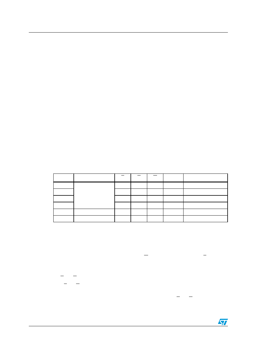
Table 2.
Operating modes
2.1
Read mode
The M48T35/Y is in the READ mode whenever W (WRITE enable) is high and E (chip
enable) is low. The unique address specified by the 15 address inputs defines which one of
the 32,768 bytes of data is to be accessed. Valid data will be available at the data I/O pins
within address access time (tAVQV) after the last address input signal is stable, providing that
the E and G access times are also satisfied.
If the E and G access times are not met, valid data will be available after the latter of the chip
enable access time (tELQV) or output enable access time (tGLQV).
The state of the eight three-state data I/O signals is controlled by E and G. If the outputs are
activated before tAVQV, the data lines will be driven to an indeterminate state until tAVQV.
Mode
VCC
E
G
W
DQ0-DQ7
Power
Deselect
4.75 to 5.5 V
or
4.5 to 5.5 V
VIH
X
High Z
Standby
WRITE
VIL
XVIL
DIN
Active
READ
VIL
VIH
DOUT
Active
READ
VIL
VIH
High Z
Active
Deselect
VSO to VPFD (min)
(1)
1.
See Table 11 on page 20 for details.
Note:
X = VIH or VIL; VSO = battery backup switchover voltage.
X
High Z
CMOS standby
Deselect
≤ VSO(1)
X
High Z
Battery backup mode
相关PDF资料 |
PDF描述 |
|---|---|
| M48T35Y-70MH1E | 0 TIMER(S), REAL TIME CLOCK, PDSO28 |
| M48T36Y-70MH1TR | 0 TIMER(S), REAL TIME CLOCK, PDSO44 |
| M48T37Y-10MH6 | 0 TIMER(S), REAL TIME CLOCK, PDSO44 |
| M48T37V-70MH1TR | 0 TIMER(S), REAL TIME CLOCK, PDSO44 |
| M48T37V-70MH1 | 0 TIMER(S), REAL TIME CLOCK, PDSO44 |
相关代理商/技术参数 |
参数描述 |
|---|---|
| M48T35-70PC1E | 制造商:STMICROELECTRONICS 制造商全称:STMicroelectronics 功能描述:5V, 256 Kbit (32 Kb x 8) TIMEKEEPER SRAM |
| M48T35-70PC1F | 制造商:STMICROELECTRONICS 制造商全称:STMicroelectronics 功能描述:5V, 256 Kbit (32 Kb x 8) TIMEKEEPER SRAM |
| M48T35-70PC1TR | 制造商:STMICROELECTRONICS 制造商全称:STMicroelectronics 功能描述:256 Kbit 32Kb x8 TIMEKEEPER SRAM |
| M48T35-70PC6 | 制造商:STMICROELECTRONICS 制造商全称:STMicroelectronics 功能描述:256 Kbit 32Kb x8 TIMEKEEPER SRAM |
| M48T35-70PC6E | 制造商:STMICROELECTRONICS 制造商全称:STMicroelectronics 功能描述:5V, 256 Kbit (32 Kb x 8) TIMEKEEPER SRAM |
发布紧急采购,3分钟左右您将得到回复。