- 您现在的位置:买卖IC网 > PDF目录69017 > M48T512V-85PM1 (STMICROELECTRONICS) 0 TIMER(S), REAL TIME CLOCK, PDIP32 PDF资料下载
参数资料
| 型号: | M48T512V-85PM1 |
| 厂商: | STMICROELECTRONICS |
| 元件分类: | 时钟/数据恢复及定时提取 |
| 英文描述: | 0 TIMER(S), REAL TIME CLOCK, PDIP32 |
| 封装: | ROHS COMPLIANT, PLASTIC, DIP-32 |
| 文件页数: | 21/23页 |
| 文件大小: | 370K |
| 代理商: | M48T512V-85PM1 |
M48T512Y, M48T512V
Operating modes
Doc ID 5747 Rev 6
7/23
2
Operating modes
The 32-pin, 600 mil hybrid DIP houses a controller chip, SRAM, quartz crystal, and a long
life lithium button cell in a single package. Figure 3 on page 6 illustrates the static memory
array and the quartz controlled clock oscillator. The clock locations contain the year, month,
date, day, hour, minute, and second in 24 hour BCD format. Corrections for 28, 29 (leap year
- compliant until the year 2100), 30, and 31 day months are made automatically. Byte
7FFF8h is the clock control register (see Table 5 on page 12). This byte controls user
access to the clock information and also stores the clock calibration setting. The seven clock
bytes (7FFFFh-7FFF9h) are not the actual clock counters; they are memory locations
consisting of BiPORT READ/WRITE memory cells within the static RAM array. The
M48T512Y/V includes a clock control circuit which updates the clock bytes with current
information once per second. The information can be accessed by the user in the same
manner as any other location in the static memory array. The M48T512Y/V also has its own
power-fail detect circuit. This control circuitry constantly monitors the supply voltage for an
out of tolerance condition. When VCC is out of tolerance, the circuit write protects the
TIMEKEEPER register data and SRAM, providing data security in the midst of unpredictable
system operation. As VCC falls, the control circuitry automatically switches to the battery,
maintaining data and clock operation until valid power is restored.
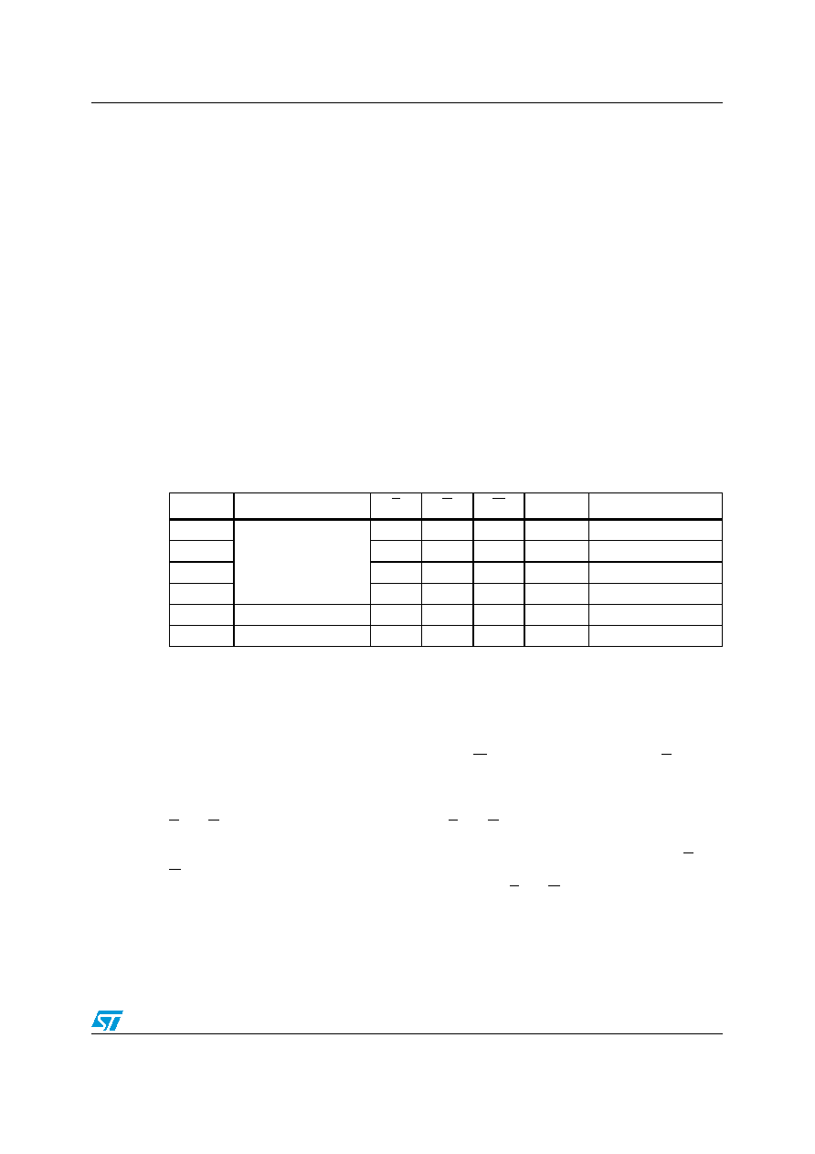
Table 2.
Operating modes
Note:
X = VIH or VIL; VSO = Battery backup switchover voltage.
2.1
READ mode
The M48T512Y/V is in the READ mode whenever W (WRITE enable) is high and E (chip
enable) is low. The unique address specified by the 19 address inputs defines which one of
the 524,288 bytes of data is to be accessed. Valid data will be available at the data I/O pins
within address access time (tAVQV) after the last address input signal is stable, providing the
E and G access times are also satisfied. If the E and G access times are not met, valid data
will be available after the latter of the chip enable access times (tELQV) or output enable
access time (tGLQV). The state of the eight three-state data I/O signals is controlled by E and
G. If the outputs are activated before tAVQV, the data lines will be driven to an indeterminate
state until tAVQV. If the address inputs are changed while E and G remain active, output data
will remain valid for output data hold time (tAXQX) but will go indeterminate until the next
address access.
Mode
VCC
E
G
W
DQ0-DQ7
Power
Deselect
4.5 to 5.5 V
or
3.0 to 3.6 V
VIH
X
High Z
Standby
WRITE
VIL
XVIL
DIN
Active
READ
VIL
VIH
DOUT
Active
READ
VIL
VIH
High Z
Active
Deselect
VSO to VPFD (min)
(1)
1.
See Table 11 on page 18 for details.
X
High Z
CMOS standby
Deselect
≤ VSO(1)
X
High Z
Battery backup mode
相关PDF资料 |
PDF描述 |
|---|---|
| M48T512V-70PM1 | REAL TIME CLOCK, PDIP32 |
| M48T513V-85PL1 | 0 TIMER(S), REAL TIME CLOCK, DMA36 |
| M48T513Y-70PM1 | 0 TIMER(S), REAL TIME CLOCK, PDIP36 |
| M48T513V-85PM1 | 0 TIMER(S), REAL TIME CLOCK, PDIP36 |
| M62320GP | 8 I/O, PIA-GENERAL PURPOSE, PDSO16 |
相关代理商/技术参数 |
参数描述 |
|---|---|
| M48T512VPM | 制造商:STMICROELECTRONICS 制造商全称:STMicroelectronics 功能描述:3.3V-5V 4 Mbit 512Kb x8 TIMEKEEPER SRAM |
| M48T512Y | 制造商:STMICROELECTRONICS 制造商全称:STMicroelectronics 功能描述:3.3V-5V 4 Mbit 512Kb x8 TIMEKEEPER SRAM |
| M48T512Y_10 | 制造商:STMICROELECTRONICS 制造商全称:STMicroelectronics 功能描述:5.0 or 3.3 V, 4 Mbit (512 Kbit x 8) TIMEKEEPER? SRAM |
| M48T512Y-70PM1 | 功能描述:实时时钟 4M (512Kx8) 70ns RoHS:否 制造商:Microchip Technology 功能:Clock, Calendar. Alarm RTC 总线接口:I2C 日期格式:DW:DM:M:Y 时间格式:HH:MM:SS RTC 存储容量:64 B 电源电压-最大:5.5 V 电源电压-最小:1.8 V 最大工作温度:+ 85 C 最小工作温度: 安装风格:Through Hole 封装 / 箱体:PDIP-8 封装:Tube |
| M48T512Y-70PM1 | 制造商:STMicroelectronics 功能描述:NVRAM 10 YR BATTERY 4MB 48T512 |
发布紧急采购,3分钟左右您将得到回复。