- 您现在的位置:买卖IC网 > PDF目录296402 > M50FW080K1 (意法半导体) 8 Mbit 1Mb x8, Uniform Block 3V Supply Firmware Hub Flash Memory PDF资料下载
参数资料
| 型号: | M50FW080K1 |
| 厂商: | 意法半导体 |
| 英文描述: | 8 Mbit 1Mb x8, Uniform Block 3V Supply Firmware Hub Flash Memory |
| 中文描述: | 8兆1兆× 8,统一座3V电源闪存固件集线器 |
| 文件页数: | 10/47页 |
| 文件大小: | 765K |
| 代理商: | M50FW080K1 |
第1页第2页第3页第4页第5页第6页第7页第8页第9页当前第10页第11页第12页第13页第14页第15页第16页第17页第18页第19页第20页第21页第22页第23页第24页第25页第26页第27页第28页第29页第30页第31页第32页第33页第34页第35页第36页第37页第38页第39页第40页第41页第42页第43页第44页第45页第46页第47页
M50FW080
18/47
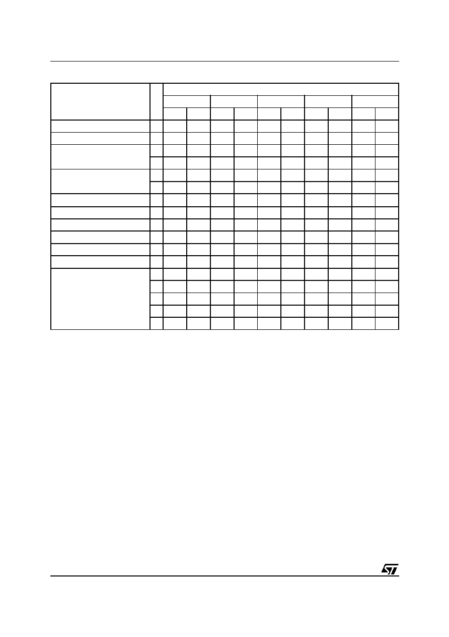
Table 9. Commands
Note: X Don’t Care, PA Program Address, PD Program Data, A1,2,3,4 Consecutive Addresses, BA Any address in the Block.
Read Memory Array. After a Read Memory Array command, read the memory as normal until another command is issued.
Read Status Register. After a Read Status Register command, read the Status Register as normal until another command is issued.
Read Electronic Signature. After a Read Electronic Signature command, read Manufacturer Code, Device Code until another com-
mand is issued.
Block Erase, Program. After these commands read the Status Register until the command completes and another command is is-
sued.
Quadruple Byte Program. This command is only valid in A/A Mux mode. Addresses A1, A2, A3 and A4 must be consecutive addresses
differing only for address bit A0 and A10. After this command read the Status Register until the command completes and another com-
mand is issued.
Chip Erase. This command is only valid in A/A Mux mode. After this command read the Status Register until the command completes
and another command is issued.
Clear Status Register. After the Clear Status Register command bits 1, 3, 4 and 5 in the Status Register are reset to ‘0’.
Program/Erase Suspend. After the Program/Erase Suspend command has been accepted, issue Read Memory Array, Read Status
Register, Program (during Erase suspend) and Program/Erase resume commands.
Program/Erase Resume. After the Program/Erase Resume command the suspended Program/Erase operation resumes, read the
Status Register until the Program/Erase Controller completes and the memory returns to Read Mode.
Invalid/Reserved. Do not use Invalid or Reserved commands.
Command
Cy
c
les
Bus Write Operations
1st
2nd
3rd
4th
5th
Addr
Data
Addr
Data
Addr
Data
Addr
Data
Addr
Data
Read Memory Array
1
X
FFh
Read Status Register
1
X
70h
Read Electronic Signature
1X
90h
1X
98h
Program
2X
40h
PA
PD
2X
10h
PA
PD
Quadruple Byte Program
5
X
30h
A1
PD
A2
PD
A3
PD
A4
PD
Chip Erase
2
X
80h
X
10h
Block Erase
2
X
20h
BA
D0h
Clear Status Register
1
X
50h
Program/Erase Suspend
1
X
B0h
Program/Erase Resume
1
X
D0h
Invalid/Reserved
1X
00h
1X
01h
1X
60h
1X
2Fh
1X
C0h
相关PDF资料 |
PDF描述 |
|---|---|
| M50FW080K1G | 8 Mbit 1Mb x8, Uniform Block 3V Supply Firmware Hub Flash Memory |
| M50FW080NB5T | 8 Mbit 1Mb x8, Uniform Block 3V Supply Firmware Hub Flash Memory |
| M50FW080NB5TG | 8 Mbit 1Mb x8, Uniform Block 3V Supply Firmware Hub Flash Memory |
| M524-012.8M | TCVCXO, CLOCK, 12.8 MHz, CMOS OUTPUT |
| M504-020.0M | TCVCXO, CLOCK, 20 MHz, CMOS OUTPUT |
相关代理商/技术参数 |
参数描述 |
|---|---|
| M50FW080K1G | 制造商:STMICROELECTRONICS 制造商全称:STMicroelectronics 功能描述:8 Mbit 1Mb x8, Uniform Block 3V Supply Firmware Hub Flash Memory |
| M50FW080K1T | 制造商:STMICROELECTRONICS 制造商全称:STMicroelectronics 功能描述:8 Mbit 1Mb x8, Uniform Block 3V Supply Firmware Hub Flash Memory |
| M50FW080K1TG | 制造商:STMICROELECTRONICS 制造商全称:STMicroelectronics 功能描述:8 Mbit 1Mb x8, Uniform Block 3V Supply Firmware Hub Flash Memory |
| M50FW080K5 | 制造商:STMICROELECTRONICS 制造商全称:STMicroelectronics 功能描述:8 Mbit 1Mb x8, Uniform Block 3V Supply Firmware Hub Flash Memory |
| M50FW080K5G | 功能描述:闪存 SERIAL FLASH RoHS:否 制造商:ON Semiconductor 数据总线宽度:1 bit 存储类型:Flash 存储容量:2 MB 结构:256 K x 8 定时类型: 接口类型:SPI 访问时间: 电源电压-最大:3.6 V 电源电压-最小:2.3 V 最大工作电流:15 mA 工作温度:- 40 C to + 85 C 安装风格:SMD/SMT 封装 / 箱体: 封装:Reel |
发布紧急采购,3分钟左右您将得到回复。