- 您现在的位置:买卖IC网 > PDF目录180233 > M5M5V416CWG-70HI 256K X 16 STANDARD SRAM, 70 ns, PBGA48 PDF资料下载
参数资料
| 型号: | M5M5V416CWG-70HI |
| 元件分类: | SRAM |
| 英文描述: | 256K X 16 STANDARD SRAM, 70 ns, PBGA48 |
| 封装: | 7 X 8.50 MM, 0.75 MM PITCH, CSP-48 |
| 文件页数: | 2/9页 |
| 文件大小: | 265K |
| 代理商: | M5M5V416CWG-70HI |
M5M5V416CWG -55HI, -70HI
2003.08.21
Ver. 7.0
4194304-BIT (262144-WORD BY 16-BIT) CMOS STATIC RAM
RENESAS LSIs
2
FUNCTION
The M5M5V416CWG is organized as 262144-words by
16-bit. These dev ices operate on a single +2.7~3.6V power
supply, and are directly TTL compatible to both input and
output. Its f ully st atic circuit needs no clocks and no
ref resh, and makes it usef ul.
The operation mode are determined by a combination of
the dev ice control inputs BC1# , BC2# , S1#, S2 , W# and
OE#. Each mode is summarized in the f unction table.
A write operation is executed whenev er the low lev el W#
ov erlaps with the low lev el BC1# and/or BC2# and the low
lev el S1# and the high lev el S2. The address(A0~A17)
must be set up bef ore the write cyc le and must be stable
during the entire cyc le.
A read operation is executed by s etting W# at a high
lev el and OE# at a low lev el while BC1# and/or BC2# and
S1# and S2 are in an activ e state(S1#=L,S2=H).
When setting BC1# at the high lev el and other pins are
in an activ e stage , upper-byt e are in a selectable mode in
which both reading and writing are enabled, and lower-byte
are in a non-selectable mode. And when setting BC2# at a
high lev el and other pins are in an activ e stage, lower-
byt e are in a selectable mode and upper-by te are in a
non-selectable mode.
When setting BC1# and BC2# at a high lev el or S1# at a
high lev el or S2 at a low lev el, the chips are in a non-
selectable mode in which both reading and writing are
disabled. In this mode, the output stage is in a high-
impedance state, allowing OR-tie with other chips and
memory expansion by BC1#, BC2# and S1#, S2.
The power supply c urrent is reduced as low as 0.2A(25°C,
ty pical), and the memory data can be held at +2V power
supply, enabling battery back-up operation during power
f ailure or power-down operation in the non-selected mode.
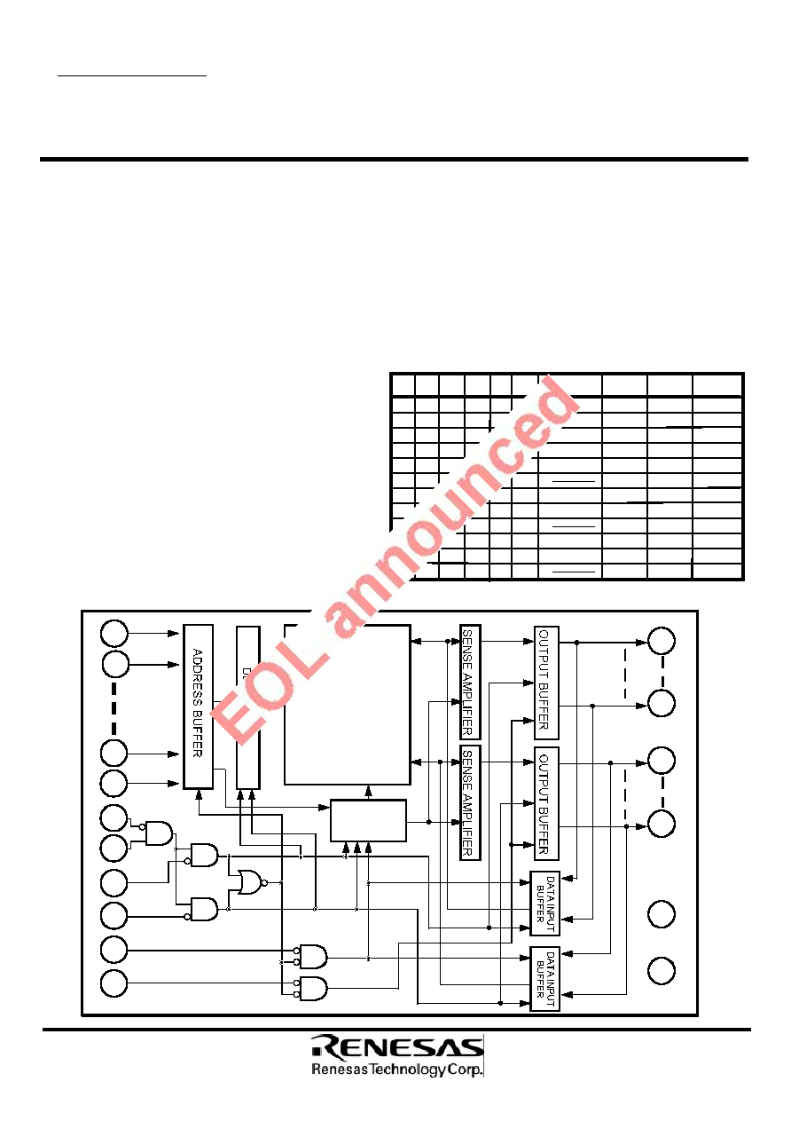
BLOCK DIAGRAM
MEMORY ARRAY
262144
WORDS
x 16
BITS
CLOCK
GENERATOR
A0
A1
A16
A17
S2
BC1#
BC2#
W#
OE#
DQ
8
DQ
1
DQ
16
DQ
9
-
Vcc
GND
S1#
FUNCTION TABLE
Mode
S2
W#
H
X
High-Z
BC1# BC2#
OE#
DQ1~8
X
Non selection
DQ9~16
Icc
High-Z
Standby
High-Z High-Z
H
X
L
H
Din
High-Z
Active
H
L
H
Read
High-Z
Dout
Active
L
H
L
Active
H
L
Active
H
L
High-Z
Active
H
L
H
High-Z
H
L
Dout
H
L
Read
Dout
Active
H
L
Din
L
X
Write
Din
Active
H
High-Z
H
High-Z High-Z
Non selection
X
H
X
Write
H
L
Write
Din
Active
X
H
L
H
Read
High-Z
Active
L
Dout
H
High-Z
S1#
H
L
X
L
X
High-Z
X
Non selection
High-Z
Standby
X
Standby
(note) "H" and "L" in this table mean VIH and VIL, respectiv ely .
"X" in this table should be "H" or "L".
相关PDF资料 |
PDF描述 |
|---|---|
| M5R24TLJ800.0000MHZ | CRYSTAL OSCILLATOR, CLOCK, 800 MHz, LVDS OUTPUT |
| M5R28TPJ-R800.0000MHZ | CRYSTAL OSCILLATOR, CLOCK, 800 MHz, PECL OUTPUT |
| M5R75XQJ0.7500MHZ | CRYSTAL OSCILLATOR, CLOCK, 0.75 MHz, PECL OUTPUT |
| M5R18THJ-R0.7500MHZ | CRYSTAL OSCILLATOR, CLOCK, 0.75 MHz, LVDS OUTPUT |
| M5R13RHJ-R0.7500MHZ | CRYSTAL OSCILLATOR, CLOCK, 0.75 MHz, LVDS OUTPUT |
相关代理商/技术参数 |
参数描述 |
|---|---|
| M5M5V416WG-70LI | 制造商:MITSUBISHI 制造商全称:Mitsubishi Electric Semiconductor 功能描述:4194304-BIT (262144-WORD BY 16-BIT) CMOS STATIC RAM |
| M5M5V4R01J-12 | 制造商:MITSUBISHI 制造商全称:Mitsubishi Electric Semiconductor 功能描述:4194304-BIT (4194304-WORD BY 1-BIT) CMOS STATIC RAM |
| M5M5V4R01J-15 | 制造商:MITSUBISHI 制造商全称:Mitsubishi Electric Semiconductor 功能描述:4194304-BIT (4194304-WORD BY 1-BIT) CMOS STATIC RAM |
| M5M5V4R04J-12 | 制造商:MITSUBISHI 制造商全称:Mitsubishi Electric Semiconductor 功能描述:4194304-BIT (1048576-WORD BY 4-BIT) CMOS STATIC RAM |
| M5M5V4R04J-15 | 制造商:MITSUBISHI 制造商全称:Mitsubishi Electric Semiconductor 功能描述:4194304-BIT (1048576-WORD BY 4-BIT) CMOS STATIC RAM |
发布紧急采购,3分钟左右您将得到回复。