- 您现在的位置:买卖IC网 > PDF目录377835 > M68AW256MN55ZB6 (意法半导体) 4 Mbit (256K x16) 3.0V Asynchronous SRAM PDF资料下载
参数资料
| 型号: | M68AW256MN55ZB6 |
| 厂商: | 意法半导体 |
| 英文描述: | 4 Mbit (256K x16) 3.0V Asynchronous SRAM |
| 中文描述: | 4兆位(256K × 16)3.0V异步SRAM |
| 文件页数: | 8/23页 |
| 文件大小: | 152K |
| 代理商: | M68AW256MN55ZB6 |
M68AW256M
8/23
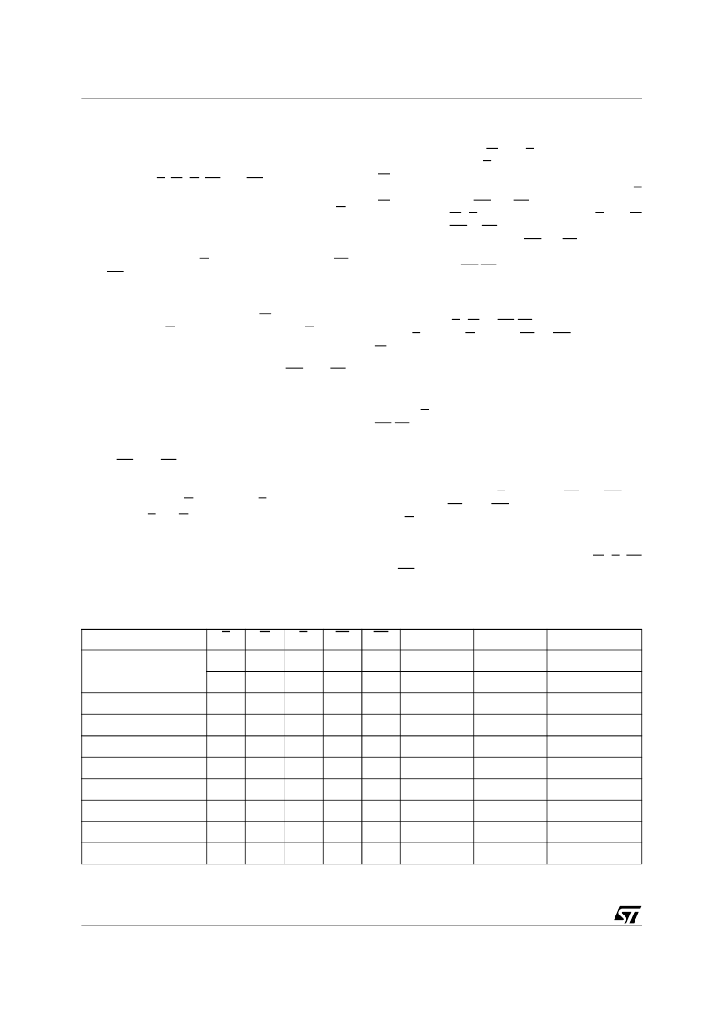
OPERATION
The device has four standard operating modes:
Output Disabled, Read, Write and Standby/Pow-
er-Down. These modes are determined by the
control inputs E, W, G, LB and UB as summarized
in
Table 2., Operating Modes
.
Output Disabled.
The Output Enable signal, G,
provides high-speed tri-state control of DQ0-
DQ15, allowing fast read/write cycles on the I/O
data bus. The device is in Output Disabled mode
when Output Enable, G, is High. In this mode, LB
and UB are Don’t care and DQ0-DQ15 are high
impedance.
Read Mode.
The M68AW256M is in the Read
mode whenever Write Enable (W) is High with
Output Enable (G) Low, and Chip Enable (E) is as-
serted.
This provides access to data from eight or sixteen,
depending on the status of the signal UB and LB,
of the 4,194,304 locations in the static memory ar-
ray, specified by the 18 address inputs.If only one
of the Byte Enable inputs is at V
IL
, the
M68AW256M is in Byte Read mode. If the two
Byte Enable inputs are at V
IL
, the M68AW256M is
in Word Read mode. So depending on the status
of the UB and LB signals, valid data will be avail-
able on the lower eight, the upper eight or all six-
teen output pins, tAVQV after the last stable
address, providing G is Low and E is Low.
If either of E or G is asserted after t
AVQV
has
elapsed, data access will be measured from the
limiting parameter (t
ELQV
, t
GLQV
or t
BLQV
) rather
than the address. Data out may be indeterminate
at t
ELQX
, t
GLQX
and t
BLQX
but data lines will always
be valid at t
AVQV
.
Write Mode.
The M68AW256M is in the Write
mode whenever the W and E are Low. Either the
Chip Enable input (E) or the Write Enable input
(W) must be de-asserted during Address
transitions for subsequent write cycles. When E
(W) is Low, and UB or LB is Low, write cycle
begins on the W (E)'s falling edge. When E and W
are Low, and UB = LB = High, write cycle begins
on the first falling edge of UB or LB. Therefore,
address setup time is referenced to Write Enable,
Chip Enable or UB/LB as t
AVWL
, t
AVEL
and t
AVBL
respectively, and is determined by the latter
occurring edge.
The Write cycle can be terminated by the earlier
rising edge of E, W or UB/LB. If the Output is en-
abled (E = Low, G = Low, LB or UB = Low), then
W will return the outputs to high impedance within
t
WLQZ
of its falling edge. Care must be taken to
avoid bus contention in this type of operation. Data
input must be valid for t
DVWH
before the rising
edge of Write Enable, or for t
DVEH
before the rising
edge of E, or for t
DVBH
before the rising edge of
UB/LB whichever occurs first, and remain valid for
t
WHDX
, t
EHDX
and t
BHDX
respectively.
Standby/Power-Down.
The M68AW256M has a
Chip Enable power down feature which invokes an
automatic standby mode whenever either Chip
Enable is de-asserted (E = High) or LB and UB are
de-asserted (LB and UB = High). An Output En-
able (G) signal provides a high speed tri-state con-
trol, allowing fast read/write cycles to be achieved
with the common I/O data bus. Operational modes
are determined by device control inputs W, E, LB
and UB as summarized in the Operating Modes ta-
ble (see Table
2
).
Table 2. Operating Modes
Note: 1. X = V
IH
or V
IL
.
Operation
E
W
G
LB
UB
DQ0-DQ7
DQ8-DQ15
Power
Deselected
(Standby/Power-Down)
V
IH
X
X
X
X
Hi-Z
Hi-Z
Standby (I
SB
)
X
X
X
V
IH
V
IH
Hi-Z
Hi-Z
Standby (I
SB
)
Lower Byte Read
V
IL
V
IH
V
IL
V
IL
V
IH
Data Output
Hi-Z
Active (I
CC
)
Lower Byte Write
V
IL
V
IL
X
V
IL
V
IH
Data Input
Hi-Z
Active (I
CC
)
Output Disabled
V
IL
V
IH
V
IH
X
X
Hi-Z
Hi-Z
Active (I
CC
)
Upper Byte Read
V
IL
V
IH
V
IL
V
IH
V
IL
Hi-Z
Data Output
Active (I
CC
)
Upper Byte Write
V
IL
V
IL
X
V
IH
V
IL
Hi-Z
Data Input
Active (I
CC
)
Word Read
V
IL
V
IH
V
IL
V
IL
V
IL
Data Output
Data Output
Active (I
CC
)
Word Write
V
IL
V
IL
X
V
IL
V
IL
Data Input
Data Input
Active (I
CC
)
Output Disabled
V
IH
X
V
IH
X
X
Hi-Z
Hi-Z
Active (I
CC
)
相关PDF资料 |
PDF描述 |
|---|---|
| M68AW256MN55ZB6E | 4 Mbit (256K x16) 3.0V Asynchronous SRAM |
| M68Z128 | 5V, 1Mbit(128Kbx8) Low Power SRAM with Output Enable(1Mb低功耗SRAM) |
| M69AW024BE | 16 Mbit (1M x16) 3V Asynchronous PSRAM |
| M69AW024BE60ZB8F | 16 Mbit (1M x16) 3V Asynchronous PSRAM |
| M7040N | 64K x 72-bit Entry NETWORK PACKET SEARCH ENGINE |
相关代理商/技术参数 |
参数描述 |
|---|---|
| M68AW256MN55ZB6E | 制造商:STMICROELECTRONICS 制造商全称:STMicroelectronics 功能描述:4 Mbit (256K x16) 3.0V Asynchronous SRAM |
| M68AW256MN55ZB6F | 制造商:STMICROELECTRONICS 制造商全称:STMicroelectronics 功能描述:4 Mbit (256K x16) 3.0V Asynchronous SRAM |
| M68AW256MN55ZB6T | 制造商:STMICROELECTRONICS 制造商全称:STMicroelectronics 功能描述:4 Mbit (256K x16) 3.0V Asynchronous SRAM |
| M68AW256MN55ZH1 | 制造商:STMICROELECTRONICS 制造商全称:STMicroelectronics 功能描述:4 Mbit (256K x16) 3.0V Asynchronous SRAM |
| M68AW256MN55ZH1E | 制造商:STMICROELECTRONICS 制造商全称:STMicroelectronics 功能描述:4 Mbit (256K x16) 3.0V Asynchronous SRAM |
发布紧急采购,3分钟左右您将得到回复。