- 您现在的位置:买卖IC网 > PDF目录359091 > M68Z128W (意法半导体) 3V, 1 Mbit 128Kb x8 Low Power SRAM with Output Enable PDF资料下载
参数资料
| 型号: | M68Z128W |
| 厂商: | 意法半导体 |
| 英文描述: | 3V, 1 Mbit 128Kb x8 Low Power SRAM with Output Enable |
| 中文描述: | 3V的,1兆位的输出128KB的x8低功耗SRAM启用 |
| 文件页数: | 2/12页 |
| 文件大小: | 96K |
| 代理商: | M68Z128W |
M68Z128W
2/12
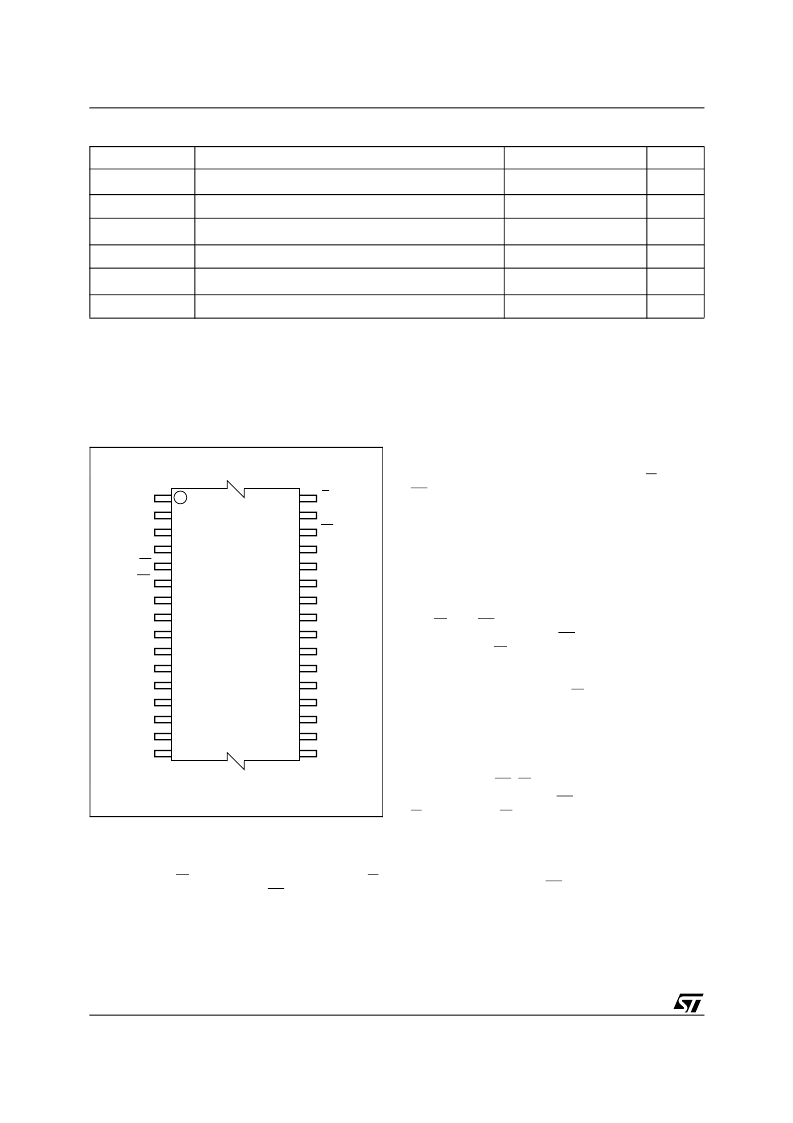
Figure 2. TSOP Connections
A1
A2
A0
DQ0
A7
A6
A5
A4
A3
A13
W
A10
E1
A8
A9
DQ7
DQ6
E2
A15
VCC
A11
G
DQ5
DQ4
DQ1
DQ2
DQ3
VSS
A16
A14
A12
NC
AI00698B
M68Z128W
8
9
1
16
17
24
25
32
Table 2. Absolute Maximum Ratings
(1)
Note: 1. Except for the rating "Operating Temperature Range", stresses above those listed in the Table "Absolute Maximum Ratings" may
cause permanent damage to the device. These are stress ratings only and operation of the device at these or any other conditions
above those indicated in the Operating sections of this specification is not implied. Exposure to Absolute Maximum Rating condi-
tions for extended periods may affect device reliability. Refer also to the STMicroelectronics SURE Program and other relevant qual-
ity documents.
2. Up to a maximum operating V
CC
of 3.6V only.
3. One output at a time, not to exceed 1 second duration.
Symbol
Parameter
Value
Unit
T
A
Ambient Operating Temperature
0 to 70
°C
T
STG
Storage Temperature
–65 to 150
°C
V
IO (2)
Input or Output Voltage
–0.5 to V
CC
+ 0.5
V
V
CC
Supply Voltage
–0.5 to 4.6
V
I
O (3)
Output Current
20
mA
P
D
Power Dissipation
1
W
READ MODE
The M68Z128W is in the Read mode whenever
Write Enable (W) is High with Output Enable (G)
Low, and both Chip Enables (E1 and E2) are as-
serted. This provides access to data from eight of
the 1,048,576 locations in the static memory array,
specified by the 17 address inputs. Valid data will
be available at the eight output pins within t
AVQV
after the last stable address, providing G is Low,
E1 is Low and E2 is High. If Chip Enable or Output
Enable access times are not met, data access will
be measured from the limiting parameter (t
E1LQV
,
t
E2HQV
, or t
GLQV
) rather than the address. Data out
may be indeterminate at t
E1LQX
, t
E2HQX
and t
GLQX
,
but data lines will always be valid at t
AVQV
.
WRITE MODE
The M68Z128W is in the Write mode whenever
the W and E1 pins are Low, with E2 High. Either
the Chip Enable inputs (E1 and E2) or the Write
Enable input (W) must be de-asserted during Ad-
dress transitions for subsequent write cycles.
Write begins with the concurrence of both Chip
Enables being active with W low. Therefore, ad-
dress setup time is referenced to Write Enable and
both Chip Enables as t
AVWL
, t
AVE1L
and t
AVE2H
re-
spectively, and is determined by the latter occur-
ring edge.
The Write cycle can be terminated by the earlier
rising edge of E1, W, or the falling edge of E2.
If the Output is enabled (E1 = Low, E2 = High and
G = Low), then W will return the outputs to high im-
pedance within t
WLQZ
of its falling edge. Care must
be taken to avoid bus contention in this type of op-
eration. Data input must be valid for t
DVWH
before
the rising edge of Write Enable, or for t
DVE1H
be-
fore the rising edge of E1 or for t
DVE2L
before the
falling edge of E2, whichever occurs first, and re-
main valid for t
WHDX
, t
E1HDX
or t
E2LDX
.
相关PDF资料 |
PDF描述 |
|---|---|
| M69AW024BL60ZB8T | 16 Mbit (1M x16) 3V Asynchronous PSRAM |
| M69AW024BL70ZB8T | 16 Mbit (1M x16) 3V Asynchronous PSRAM |
| M69AW024B | 16 Mbit (1M x16) 3V Asynchronous PSRAM |
| M69AW048B | 32 Mbit (2M x16) 3V Asynchronous PSRAM |
| M69AW048BL70ZB8 | 32 Mbit (2M x16) 3V Asynchronous PSRAM |
相关代理商/技术参数 |
参数描述 |
|---|---|
| M68Z128W-70N1 | 功能描述:RAM其它 4M (128Kx8) 70ns RoHS:否 制造商:Freescale Semiconductor 封装:Tray |
| M68Z128W-70N1T | 制造商:STMICROELECTRONICS 制造商全称:STMicroelectronics 功能描述:3V, 1 Mbit 128Kb x8 Low Power SRAM with Output Enable |
| M68Z128WN | 制造商:STMICROELECTRONICS 制造商全称:STMicroelectronics 功能描述:3V, 1 Mbit 128Kb x8 Low Power SRAM with Output Enable |
| M68Z512 | 制造商:STMICROELECTRONICS 制造商全称:STMicroelectronics 功能描述:4 Mbit 512Kb x8 Low Power SRAM with Output Enable |
| M68Z512-70NC1T | 制造商:STMICROELECTRONICS 制造商全称:STMicroelectronics 功能描述:4 Mbit 512Kb x8 Low Power SRAM with Output Enable |
发布紧急采购,3分钟左右您将得到回复。