- 您现在的位置:买卖IC网 > PDF目录80567 > M902-01I156.2500LF (INTEGRATED DEVICE TECHNOLOGY INC) 156.25 MHz, OTHER CLOCK GENERATOR, CQCC36 PDF资料下载
参数资料
| 型号: | M902-01I156.2500LF |
| 厂商: | INTEGRATED DEVICE TECHNOLOGY INC |
| 元件分类: | 时钟产生/分配 |
| 英文描述: | 156.25 MHz, OTHER CLOCK GENERATOR, CQCC36 |
| 封装: | 9 X 9 MM, CERAMIC, LCC-36 |
| 文件页数: | 4/8页 |
| 文件大小: | 328K |
| 代理商: | M902-01I156.2500LF |
M902-01 Datasheet Rev 2.1
4 of 8
Revised 24Jun2004
I n te g r at ed C i rcui t Syste m s , Inc. ● Ne tw or kin g & C o mmun ica t io ns ● ww w. ic st.c om ● tel (5 08 ) 8 52-5 4 0 0
M902-01
VCSO BASED GBE CLOCK GENERATOR
Prod uct Data Sh eet
APPLICATION INFORMATION
This section includes information on the optional
external crystal and on the external loop filter.
External Crystal Specifications
If an external crystal is used with the on-chip crystal
oscillator circuit (XTAL OSC), the external crystal
should have the following general specifications:
The external crystal will be applied to the XTAL_1 / REF_IN
and XTAL_2 input pins. External crystal load capacitors
are also required.
Recommended External Crystal Configuration
XTAL= 25 or 30 MHz, Load Capacitance Specification = 18 pF
C1
= 27 pF
C2
= 33 pF
External load capacitors C1 and C2 present a load of 15 pf
to the crystal (they are seen in series by the crystal through
the common ground connection). With the additional of PCB
trace capacitance and M902-01 input capacitance, the total
load to the crystal is about 18 pf.
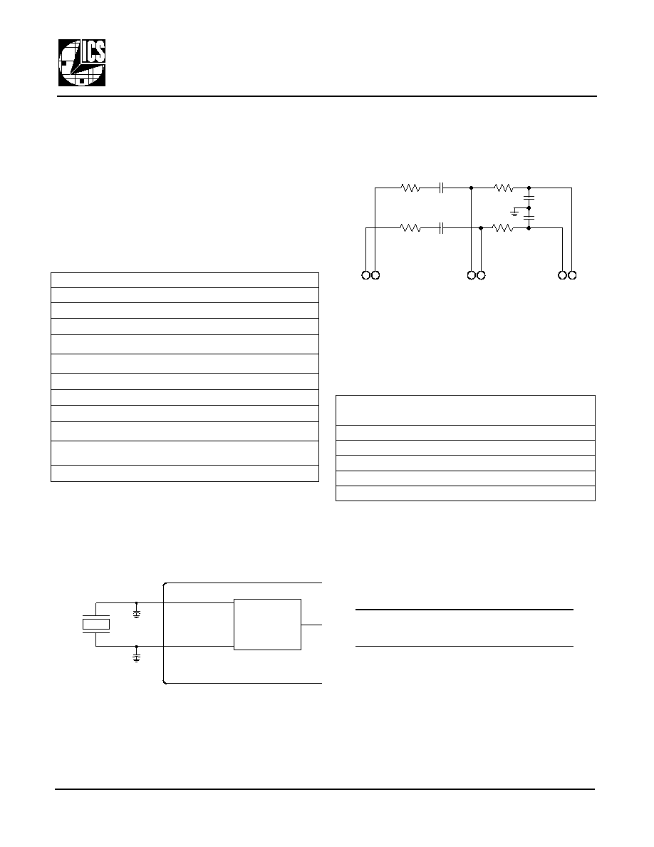
External Loop Filter
To provide stable PLL operation, and thereby a low jitter
output clock, the M902-01 requires the use of an
external loop filter. This is provided via the provided
filter pins (see Figure 5).
Figure 5: External Loop Filter
The loop filter is implemented as a differential circuit
to minimize system noise interference. Due to the
differential signal path design, the implementation
requires two identical complementary RC filters as
shown here. See Table 4, External Loop Filter
Component Values, below.
additional product information.
Crystal Specifications
Parameter
Min Typ Max Unit
Crystal Type
AT-cut quartz
Mode of Oscillation
Fundamental
f0
Nominal Frequency Range
16
40
MHz
f/f0
Frequency Tolerance @+25 oC 1
Note 1: These frequency tolerance specifications are suitable for
a
±100 ppm clock output frequency requirement.
±15
ppm
f/f
C / TA
Frequency Stability -40 to +85 oC 1
±50
ppm
f/f0 / y Aging, per year (first) @+25 oC 1
±5
ppm
ESR
Equivalent Series Resistance
50
C
S
Shunt Capacitance
7
pF
Spurious Response (non-harmonic)
-40 dBc
C
L
Load Capacitance,
parallel load resonant
16
32
pF
P0
Drive Level
0.1
1.0
mW
XTAL_2
XTAL
XTAL OSC
M9xx-0x
XTAL_1 / REF_IN
C1
C2
M902-01
External Loop Filter Component Values
PLL Bandwidth
(kHz)
Damping
Factor
R loop
(k
)
C loop
(
F)
R post
(k
)
C post
(pF)
0.5
3.0
1.5
4.70
20
150
1.5 1
Note 1: Optimum loop bandwidth when using an external reference
crystal. Will help to attenuate interference on the crystal’s
sinusoidal clock waveform and therefore will minimize
device output clock jitter.
3.3
4.7
1.00
10
150
2.1 2
Note 2: Alternative loop filter setting when using an external refer-
ence crystal. Smaller C loop lowers loop damping factor with
negligible increase in output jitter.
1.1
4.7
0.10
10
150
6.4
4.5
20.0
0.10
20
270
10.6
3
Note 3: Optimum loop bandwidth when using an external reference
crystal oscillator. The square wave clock reference does not
require as much jitter attenuation, which allows for a wider
loop bandwidth and improved system noise tolerance.
4.2
33.0
0.03
20
120
C
POST
C
POST
VC
nVC
R
POST
nOP_OUT
OP_OUT
R
POST
R
LOOP
R
LOOP
C
LOOP
C
LOOP
OP_IN
nOP_IN
相关PDF资料 |
PDF描述 |
|---|---|
| M906-01I190.0000 | 190 MHz, OTHER CLOCK GENERATOR, CQCC36 |
| MK1442-01SLF | 100 MHz, PROC SPECIFIC CLOCK GENERATOR, PDSO16 |
| MK2049-45ASITR | 125 MHz, OTHER CLOCK GENERATOR, PDSO20 |
| MK2751-01STR | 66 MHz, VIDEO CLOCK GENERATOR, PDSO16 |
| MK3712STR | 27 MHz, OTHER CLOCK GENERATOR, PDSO8 |
相关代理商/技术参数 |
参数描述 |
|---|---|
| M902-01I187.5000 | 制造商:ICS 制造商全称:ICS 功能描述:VCSO BASED GBE CLOCK GENERATOR |
| M9022 | 制造商:Tamura Corporation of America 功能描述: |
| M902-2243 | 制造商:TE Connectivity 功能描述:CONNECTOR |
| M9023 | 制造商:Tamura Corporation of America 功能描述: |
| M90-25042-10SL | 功能描述:环形MIL规格工具、五金与附件 CAP W/CHAIN EXT THRD 5/8-24UNEF-2B THREAD RoHS:否 制造商:Amphenol Industrial MIL 类型:MIL-DTL-5015 系列:97 产品类型:Dummy Receptacles 用于:97 Series Plugs |
发布紧急采购,3分钟左右您将得到回复。