- 您现在的位置:买卖IC网 > PDF目录229297 > M93C06-MB6G (STMICROELECTRONICS) 16 X 16 MICROWIRE BUS SERIAL EEPROM, DSO8 PDF资料下载
参数资料
| 型号: | M93C06-MB6G |
| 厂商: | STMICROELECTRONICS |
| 元件分类: | PROM |
| 英文描述: | 16 X 16 MICROWIRE BUS SERIAL EEPROM, DSO8 |
| 封装: | 2 X 3 MM, LEAD FREE, MLP-8 |
| 文件页数: | 3/31页 |
| 文件大小: | 533K |
| 代理商: | M93C06-MB6G |
第1页第2页当前第3页第4页第5页第6页第7页第8页第9页第10页第11页第12页第13页第14页第15页第16页第17页第18页第19页第20页第21页第22页第23页第24页第25页第26页第27页第28页第29页第30页第31页
11/31
M93C86, M93C76, M93C66, M93C56, M93C46, M93C06
READY/BUSY STATUS
While the Write or Erase cycle is underway, for a
WRITE, ERASE, WRAL or ERAL instruction, the
Busy signal (Q=0) is returned whenever Chip Se-
lect Input (S) is driven High. (Please note, though,
that there is an initial delay, of tSLSH, before this
status information becomes available). In this
state, the M93Cx6 ignores any data on the bus.
When the Write cycle is completed, and Chip Se-
lect Input (S) is driven High, the Ready signal
(Q=1) indicates that the M93Cx6 is ready to re-
ceive the next instruction. Serial Data Output (Q)
remains set to 1 until the Chip Select Input (S) is
brought Low or until a new start bit is decoded.
COMMON I/O OPERATION
Serial Data Output (Q) and Serial Data Input (D)
can be connected together, through a current lim-
iting resistor, to form a common, single-wire data
bus. Some precautions must be taken when oper-
ating the memory in this way, mostly to prevent a
short circuit current from flowing when the last ad-
dress bit (A0) clashes with the first data bit on Se-
rial Data Output (Q). Please see the application
note AN394 for details.
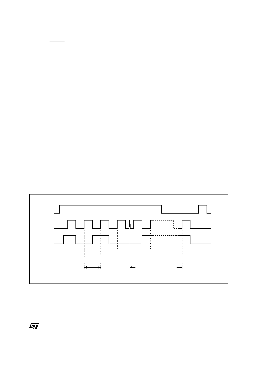
CLOCK PULSE COUNTER
In a noisy environment, the number of pulses re-
ceived on Serial Clock (C) may be greater than the
number delivered by the master (the microcontrol-
ler). This can lead to a misalignment of the instruc-
tion of one or more bits (as shown in Figure 7.) and
may lead to the writing of erroneous data at an er-
roneous address.
To combat this problem, the M93Cx6 has an on-
chip counter that counts the clock pulses from the
start bit until the falling edge of the Chip Select In-
put (S). If the number of clock pulses received is
not the number expected, the WRITE, ERASE,
ERAL or WRAL instruction is aborted, and the
contents of the memory are not modified.
The number of clock cycles expected for each in-
struction, and for each member of the M93Cx6
example, a Write Data to Memory (WRITE) in-
struction on the M93C56 (or M93C66) expects 20
clock cycles (for the x8 organization) from the start
bit to the falling edge of Chip Select Input (S). That
is:
1 Start bit
+ 2 Op-code bits
+ 9 Address bits
+ 8 Data bits
Figure 7. Write Sequence with One Clock Glitch
AI01395
S
An-1
C
D
WRITE
START
D0
"1"
"0"
An
Glitch
An-2
ADDRESS AND DATA
ARE SHIFTED BY ONE BIT
相关PDF资料 |
PDF描述 |
|---|---|
| MT48LC4M16A2F4-6IT:G | 4M X 16 SYNCHRONOUS DRAM, 5.5 ns, PBGA54 |
| MT46V32M8FG-6TIT:G | 32M X 8 DDR DRAM, 0.7 ns, PBGA60 |
| MT46V32M8BG-6AT:G | 32M X 8 DDR DRAM, 0.7 ns, PBGA60 |
| M29F800FB55N3E2 | 512K X 16 FLASH 5V PROM, 55 ns, PDSO48 |
| MC12L1NZGF | ROTARY SWITCH-12POSITIONS, SP12T, LATCHED, 0.25A, 28VDC, PANEL MOUNT-THREADED |
相关代理商/技术参数 |
参数描述 |
|---|---|
| M93C06MN | 制造商:STMICROELECTRONICS 制造商全称:STMicroelectronics 功能描述:16Kbit, 8Kbit, 4Kbit, 2Kbit, 1Kbit and 256bit 8-bit or 16-bit wide |
| M93C06-MN6 | 功能描述:电可擦除可编程只读存储器 256 (32x8 or 16x16) RoHS:否 制造商:Atmel 存储容量:2 Kbit 组织:256 B x 8 数据保留:100 yr 最大时钟频率:1000 KHz 最大工作电流:6 uA 工作电源电压:1.7 V to 5.5 V 最大工作温度:+ 85 C 安装风格:SMD/SMT 封装 / 箱体:SOIC-8 |
| M93C06-MN6T | 功能描述:电可擦除可编程只读存储器 256 (32x8 or 16x16) RoHS:否 制造商:Atmel 存储容量:2 Kbit 组织:256 B x 8 数据保留:100 yr 最大时钟频率:1000 KHz 最大工作电流:6 uA 工作电源电压:1.7 V to 5.5 V 最大工作温度:+ 85 C 安装风格:SMD/SMT 封装 / 箱体:SOIC-8 |
| M93C06-WBN6 | 功能描述:电可擦除可编程只读存储器 256 (32x8 or 16x16) RoHS:否 制造商:Atmel 存储容量:2 Kbit 组织:256 B x 8 数据保留:100 yr 最大时钟频率:1000 KHz 最大工作电流:6 uA 工作电源电压:1.7 V to 5.5 V 最大工作温度:+ 85 C 安装风格:SMD/SMT 封装 / 箱体:SOIC-8 |
| M93C06-WMN6 | 功能描述:电可擦除可编程只读存储器 256 (32x8 or 16x16) RoHS:否 制造商:Atmel 存储容量:2 Kbit 组织:256 B x 8 数据保留:100 yr 最大时钟频率:1000 KHz 最大工作电流:6 uA 工作电源电压:1.7 V to 5.5 V 最大工作温度:+ 85 C 安装风格:SMD/SMT 封装 / 箱体:SOIC-8 |
发布紧急采购,3分钟左右您将得到回复。