- 您现在的位置:买卖IC网 > PDF目录359112 > M93C46DS (意法半导体) 16Kbit, 8Kbit, 4Kbit, 2Kbit, 1Kbit and 256bit 8-bit or 16-bit wide PDF资料下载
参数资料
| 型号: | M93C46DS |
| 厂商: | 意法半导体 |
| 英文描述: | 16Kbit, 8Kbit, 4Kbit, 2Kbit, 1Kbit and 256bit 8-bit or 16-bit wide |
| 中文描述: | 16Kbit,8Kbit,4Kbit,2Kbit,1Kbit和256 8位或16位全 |
| 文件页数: | 11/31页 |
| 文件大小: | 611K |
| 代理商: | M93C46DS |
第1页第2页第3页第4页第5页第6页第7页第8页第9页第10页当前第11页第12页第13页第14页第15页第16页第17页第18页第19页第20页第21页第22页第23页第24页第25页第26页第27页第28页第29页第30页第31页
11/31
M93C86, M93C76, M93C66, M93C56, M93C46
READY/BUSY STATUS
While the Write or Erase cycle is underway, for a
WRITE, ERASE, WRAL or ERAL instruction, the
Busy signal (Q=0) is returned whenever Chip Se-
lect Input (S) is driven High. (Please note, though,
that there is an initial delay, of t
SLSH
, before this
status information becomes available). In this
state, the M93Cx6 ignores any data on the bus.
When the Write cycle is completed, and Chip Se-
lect Input (S) is driven High, the Ready signal
(Q=1) indicates that the M93Cx6 is ready to re-
ceive the next instruction. Serial Data Output (Q)
remains set to 1 until the Chip Select Input (S) is
brought Low or until a new start bit is decoded.
COMMON I/O OPERATION
Serial Data Output (Q) and Serial Data Input (D)
can be connected together, through a current lim-
iting resistor, to form a common, single-wire data
bus. Some precautions must be taken when oper-
ating the memory in this way, mostly to prevent a
short circuit current from flowing when the last ad-
dress bit (A0) clashes with the first data bit on Se-
rial Data Output (Q). Please see the application
note
AN394
for details.
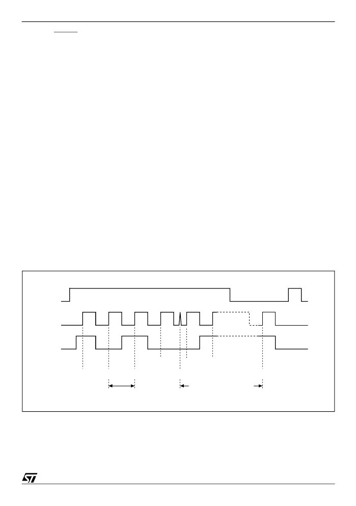
CLOCK PULSE COUNTER
In a noisy environment, the number of pulses re-
ceived on Serial Clock (C) may be greater than the
number delivered by the master (the microcontrol-
ler). This can lead to a misalignment of the instruc-
tion of one or more bits (as shown in
Figure 7.
) and
may lead to the writing of erroneous data at an er-
roneous address.
To combat this problem, the M93Cx6 has an on-
chip counter that counts the clock pulses from the
start bit until the falling edge of the Chip Select In-
put (S). If the number of clock pulses received is
not the number expected, the WRITE, ERASE,
ERAL or WRAL instruction is aborted, and the
contents of the memory are not modified.
The number of clock cycles expected for each in-
struction, and for each member of the M93Cx6
family, are summarized in
Table 5.
to
Table 7.
. For
example, a Write Data to Memory (WRITE) in-
struction on the M93C56 (or M93C66) expects 20
clock cycles (for the x8 organization) from the start
bit to the falling edge of Chip Select Input (S). That
is:
1 Start bit
+ 2 Op-code bits
+ 9 Address bits
+ 8 Data bits
Figure 7. Write Sequence with One Clock Glitch
AI01395
S
An-1
C
D
WRITE
START
D0
"1"
"0"
An
Glitch
An-2
ADDRESS AND DATA
ARE SHIFTED BY ONE BIT
相关PDF资料 |
PDF描述 |
|---|---|
| M93C46BN | 16Kbit, 8Kbit, 4Kbit, 2Kbit, 1Kbit and 256bit 8-bit or 16-bit wide |
| M93C46-WMN | 16Kbit, 8Kbit, 4Kbit, 2Kbit and 1Kbit (8-bit or 16-bit wide) MICROWIRE Serial Access EEPROM |
| M93S56-BN3G | 4Kbit, 2Kbit and 1Kbit 16-bit wide MICROWIRE Serial Access EEPROM with Block Protection |
| M93S56-MN3T | 4Kbit, 2Kbit and 1Kbit 16-bit wide MICROWIRE Serial Access EEPROM with Block Protection |
| M93S56-MN3TG | 4Kbit, 2Kbit and 1Kbit 16-bit wide MICROWIRE Serial Access EEPROM with Block Protection |
相关代理商/技术参数 |
参数描述 |
|---|---|
| M93C46-DS | 制造商:STMICROELECTRONICS 制造商全称:STMicroelectronics 功能描述:16Kbit, 8Kbit, 4Kbit, 2Kbit and 1Kbit (8-bit or 16-bit wide) MICROWIRE Serial Access EEPROM |
| M93C46-DS3 | 制造商:STMICROELECTRONICS 制造商全称:STMicroelectronics 功能描述:16Kbit, 8Kbit, 4Kbit, 2Kbit and 1Kbit (8-bit or 16-bit wide) MICROWIRE Serial Access EEPROM |
| M93C46-DS3G/S | 制造商:STMICROELECTRONICS 制造商全称:STMicroelectronics 功能描述:16 Kbit, 8 Kbit, 4 Kbit, 2 Kbit and 1 Kbit (8-bit or 16-bit wide) MICROWIRE㈢ serial access EEPROM |
| M93C46-DS3G/W | 制造商:STMICROELECTRONICS 制造商全称:STMicroelectronics 功能描述:16 Kbit, 8 Kbit, 4 Kbit, 2 Kbit and 1 Kbit (8-bit or 16-bit wide) MICROWIRE㈢ serial access EEPROM |
| M93C46-DS3P/S | 制造商:STMICROELECTRONICS 制造商全称:STMicroelectronics 功能描述:16 Kbit, 8 Kbit, 4 Kbit, 2 Kbit and 1 Kbit (8-bit or 16-bit wide) MICROWIRE㈢ serial access EEPROM |
发布紧急采购,3分钟左右您将得到回复。