- 您现在的位置:买卖IC网 > PDF目录380325 > MAS3519F (MICRONAS SEMICONDUCTOR HOLDING AG) MAS 35x9F MPEG Layer 2/3, AAC Audio Decoder, G.729 Annex A Codec PDF资料下载
参数资料
| 型号: | MAS3519F |
| 厂商: | MICRONAS SEMICONDUCTOR HOLDING AG |
| 元件分类: | Codec |
| 英文描述: | MAS 35x9F MPEG Layer 2/3, AAC Audio Decoder, G.729 Annex A Codec |
| 中文描述: | 新加坡金融管理局35x9F的MPEG 2 / 3层,AAC音频解码器,G.729的附件A编解码器 |
| 文件页数: | 22/92页 |
| 文件大小: | 1186K |
| 代理商: | MAS3519F |
第1页第2页第3页第4页第5页第6页第7页第8页第9页第10页第11页第12页第13页第14页第15页第16页第17页第18页第19页第20页第21页当前第22页第23页第24页第25页第26页第27页第28页第29页第30页第31页第32页第33页第34页第35页第36页第37页第38页第39页第40页第41页第42页第43页第44页第45页第46页第47页第48页第49页第50页第51页第52页第53页第54页第55页第56页第57页第58页第59页第60页第61页第62页第63页第64页第65页第66页第67页第68页第69页第70页第71页第72页第73页第74页第75页第76页第77页第78页第79页第80页第81页第82页第83页第84页第85页第86页第87页第88页第89页第90页第91页第92页
MAS 35x9F
DATA SHEET
22
June 30, 2004; 6251-505-1DS
Micronas
3. Controlling
3.1. I
2
C Interface
Controlling between the MAS 35x9F and the external
controller is done via an I
2
C slave interface.
3.1.1. Device Address
The device addresses are 3C/3E
hex
(device write
“DW”) and 3D/3F
hex
(device read, “DR”) as shown in
Table 3–1. The device address pair 3C/3D
hex
applies if
the DVS pin is connected to VSS, the device address
pair 3E/3F
hex
applies if the DVS pin is connected to
I2CVDD.
I
2
C clock synchronization is used to slow down the
interface if required.
3.1.2. I
2
C Registers and Subaddresses
The interface uses one level of subaddresses. The
MAS 35x9F interface has 7 subaddresses allocated
for the corresponding I
2
C registers. The registers can
be divided into three categories as shown in Table 3–
2.
The address 6A
hex
is used for basic control, i.e. reset
and task select. The other addresses are used for data
transfer from/to the MAS 35x9F.
The I
2
C registers of the MAS 35x9F are 16 bits wide,
the MSB is denoted as bit[15]. Transmissions via I
2
C
bus have to take place in 16-bit words (two byte trans-
fers, MSB sent first); thus, for each register access,
two 8-bit data words must be sent/received via I
2
C
bus.
3.1.3. Naming Convention
The description of the various controller commands
uses the following formalism:
–
Abbreviations
used in the following descriptions:
a
address
d
data value
n
count value
o
offset value
r
register number
x
don’t care
– Memory addresses, like D1:89f, are always in hexa-
decimal notation.
– A data value is split into 4-bit nibbles which are
numbered beginning with 0 for the least significant
nibble.
– Data values in nibbles are always shown in hexa-
decimal notation.
– A hexadecimal 20-bit number
d
is written, e.g. as
d
= 17C63
hex
, its five nibbles are
d0 = 3
hex
, d1 = 6
hex
, d2 = C
hex
, d3 = 7
hex
, and
d4 = 1
hex
.
–
Variables
used in the following descriptions:
I2C address:
DW3C/3E
hex
I
2
C device write
DR3D/3F
hex
I
2
C device read
DSP core:
data_write68
hex
DSP data write
data_read69
hex
DSP data read
Codec:
codec_write6C
hex
codec write
codec_read6D
hex
codec read
–
Bus signals
S
Start
P
Stop
A
ACK = Acknowledge
N
NAK = Not acknowledge
W Wait = I
2
C clock line is held low
while the MAS 35x9F is processing
the current I
2
C command
–
Symbols
in the telegram examples
<
Start Condition
>
Stop
dd
data bytes
xx
ignore
All telegram numbers are hexadecimal, data origi-
nating from the MAS 35x9F are represented as gray
letters.
Example:
<DW 68
dd dd
>
<DW 69 <DR
dd dd
>
read data from DSP
write data to DSP
Fig. 3–1 shows I
2
C bus protocols for write and read
operations of the interface; the read operations require
an extra start condition and repetition of the chip
address with the device read command (DR). Fields
with signals/data originating from the MAS 35x9F are
marked by a gray background.
Note:
In some cases the data reading process must
be concluded by a NAK condition.
3.2. Direct Configuration Registers
The task selection of the DSP and the DC/DC convert-
ers are controlled in the direct configuration registers
CONTROL, DCCF, and DCFR.
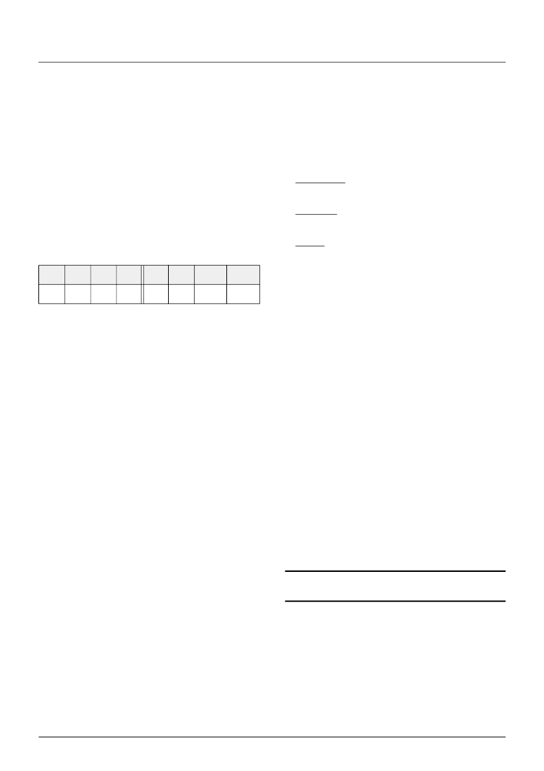
Table 3–1:
I
2
C device address
A7
A6
A5
A4
A3
A2
A1
W/R
0
0
1
1
1
1
DVS
0/1
相关PDF资料 |
PDF描述 |
|---|---|
| MAS3529F | MAS 35x9F MPEG Layer 2/3, AAC Audio Decoder, G.729 Annex A Codec |
| MAS3539F | MAS 35x9F MPEG Layer 2/3, AAC Audio Decoder, G.729 Annex A Codec |
| MAS3549F | MAS 35x9F MPEG Layer 2/3, AAC Audio Decoder, G.729 Annex A Codec |
| MAS3587F | MPEG Layer 3 Audio Encoder/Decoder |
| MAS7848L | RDS MODEM / MANCHESTER DECODER |
相关代理商/技术参数 |
参数描述 |
|---|---|
| MAS3529F | 制造商:MICRONAS 制造商全称:MICRONAS 功能描述:MAS 35x9F MPEG Layer 2/3, AAC Audio Decoder, G.729 Annex A Codec |
| MAS3539F | 制造商:MICRONAS 制造商全称:MICRONAS 功能描述:MAS 35x9F MPEG Layer 2/3, AAC Audio Decoder, G.729 Annex A Codec |
| MAS3549F | 制造商:MICRONAS 制造商全称:MICRONAS 功能描述:MAS 35x9F MPEG Layer 2/3, AAC Audio Decoder, G.729 Annex A Codec |
| MAS3559F | 制造商:MICRONAS 制造商全称:MICRONAS 功能描述:MAS 35x9F MPEG Layer 2/3, AAC Audio Decoder, G.729 Annex A Codec |
| MAS3587F | 制造商:未知厂家 制造商全称:未知厂家 功能描述:MPEG Layer 3 Audio Encoder/Decoder |
发布紧急采购,3分钟左右您将得到回复。