- 您现在的位置:买卖IC网 > PDF目录380325 > MAS9090B (MICRONAS SEMICONDUCTOR HOLDING AG) LOW VOLTAGE 14-BIT LINEAR CODEC PDF资料下载
参数资料
| 型号: | MAS9090B |
| 厂商: | MICRONAS SEMICONDUCTOR HOLDING AG |
| 元件分类: | Codec |
| 英文描述: | LOW VOLTAGE 14-BIT LINEAR CODEC |
| 中文描述: | 低电压14位线性编解码器 |
| 文件页数: | 19/30页 |
| 文件大小: | 459K |
| 代理商: | MAS9090B |
第1页第2页第3页第4页第5页第6页第7页第8页第9页第10页第11页第12页第13页第14页第15页第16页第17页第18页当前第19页第20页第21页第22页第23页第24页第25页第26页第27页第28页第29页第30页
DA9090B.001
January 14, 1998
19
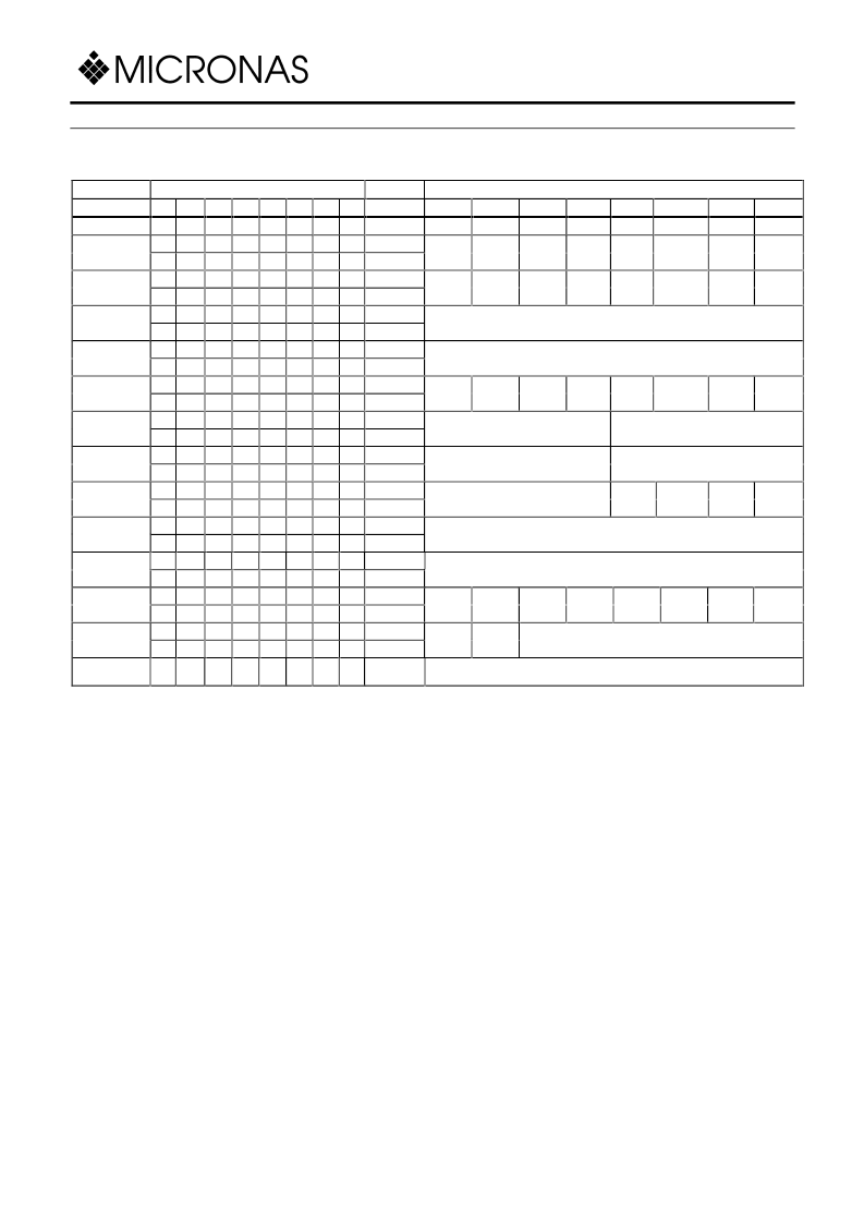
FUNCTIONAL DESCRIPTION
N
Registers
Register Map
Register
Address Byte
5
4
X
X
0
0
0
0
0
0
0
0
0
1
0
1
0
1
0
1
1
0
1
0
1
0
1
0
1
1
1
1
1
1
1
1
0
0
0
0
0
0
0
0
0
1
0
1
0
1
0
1
X
X
I/O
Data Byte
4
7
P
P
P
P
P
P
P
P
P
P
P
P
P
P
P
P
P
P
P
P
P
P
P
P
P
X
6
X
0
0
0
0
0
0
0
0
0
0
0
0
0
0
0
0
1
1
1
1
1
1
1
1
X
3
X
0
0
1
1
0
0
1
1
0
0
1
1
0
0
1
1
0
0
1
1
0
0
1
1
X
2
X
0
1
0
1
0
1
0
1
0
1
0
1
0
1
0
1
0
1
0
1
0
1
0
1
X
1
0
1
1
1
1
1
1
1
1
1
1
1
1
1
1
1
1
1
1
1
1
1
1
1
1
X
0
X
X
X
X
X
X
X
X
X
X
X
X
X
X
X
X
X
X
X
X
X
X
X
X
X
X
7
6
5
3
2
1
0
Power
CR0
Write
Read
Write
Read
Write
Read
Write
Read
Write
Read
Write
Read
Write
Read
Write
Read
Write
Read
Write
Read
Write
Read
Write
Read
F1
F0
CM
MA
IA
FF
B7
DL
CR1
DM1
DM0
DO
MR
MX
EN
TS
SV
CR2
Input data [0:7]
CR3
Output data [0:7]
CR4
VS
TE
SI
OE1
OE2
RTE
HPR
SE
CR5
TX gain [4:7]
Side tone gain [0:3]
CR6
SP1 gain [4:7]
SP2 gain [0:3]
CR7
Tone gain [4:7]
F1
F2
SN
DE
CR8
Binary word used for calculating f1
CR9
Binary word used for calculating f2
CR10
POR
SCA
HPT
EXT
LI
LO
DFT
HFT
CR11
BE
BI
Duty cycle for BZ (0:5)
CR14
For testing purposes only
Address byte bits:
Bit 0 reserved for future extensions
Bit 1 indicates the presence of a second byte. If cleared indicates single byte power up/down command
Bit 2 is write/read select bit
Bits 6 to 3 contain the address of register
Registers CR12, CR13, CR15 are not accessible
MSB bit (bit 7) of the address and data byte is always clocked first into or out from CI and CO pins
Bit 7 ‘P’ controls the power up/down state of the chip. P = 1 means power down
Data bits:
All registers are cleared during power on reset or by writing to bit POR of CR10
Default value for all bits is zero.
Notice the difference between power down and POR. Registers can be written in both power down/up states and
they retain their values in power down. Both data and control registers are cleared when POR bit (in CR10) is
written high or during power on reset (i.e. Vcc transition from 0 volts to 3-5 volts).
相关PDF资料 |
PDF描述 |
|---|---|
| MAS9090BJ | LOW VOLTAGE 14-BIT LINEAR CODEC |
| MAS9090BJ-T | LOW VOLTAGE 14-BIT LINEAR CODEC |
| MAS9090BS | LOW VOLTAGE 14-BIT LINEAR CODEC |
| MAS9128A | LDO Voltage Regulator IC |
| MAS9128AS | LDO Voltage Regulator IC |
相关代理商/技术参数 |
参数描述 |
|---|---|
| MAS9090BJ | 制造商:MICRONAS 制造商全称:MICRONAS 功能描述:LOW VOLTAGE 14-BIT LINEAR CODEC |
| MAS9090BJ-T | 制造商:MICRONAS 制造商全称:MICRONAS 功能描述:LOW VOLTAGE 14-BIT LINEAR CODEC |
| MAS9090BS | 制造商:MICRONAS 制造商全称:MICRONAS 功能描述:LOW VOLTAGE 14-BIT LINEAR CODEC |
| MAS9090BS-T | 制造商:MICRONAS 制造商全称:MICRONAS 功能描述:LOW VOLTAGE 14-BIT LINEAR CODEC |
| MAS9116 | 制造商:MAS 制造商全称:MAS 功能描述:Stereo Digital Volume Control |
发布紧急采购,3分钟左右您将得到回复。