- 您现在的位置:买卖IC网 > PDF目录2007 > MAX038CWP+ (Maxim Integrated Products)IC GEN WAVEFORM HI-FREQ 20-SOIC PDF资料下载
参数资料
| 型号: | MAX038CWP+ |
| 厂商: | Maxim Integrated Products |
| 文件页数: | 3/17页 |
| 文件大小: | 0K |
| 描述: | IC GEN WAVEFORM HI-FREQ 20-SOIC |
| 标准包装: | 36 |
| 频率: | 0.1Hz ~ 20MHz |
| 电源电压: | 4.75 V ~ 5.25 V |
| 电流 - 电源: | 45mA |
| 工作温度: | 0°C ~ 70°C |
| 封装/外壳: | 20-SOIC(0.295",7.50mm 宽) |
| 包装: | 管件 |
| 供应商设备封装: | 20-SOIC W |
| 安装类型: | 表面贴装 |
With FADJ disabled, the output frequency can still be
changed by modulating IIN.
Swept Frequency Operation
The output frequency can be swept by applying a vary-
ing signal to IIN or FADJ. IIN has a wider range, slightly
slower response, lower temperature coefficient, and
requires a single polarity current source. FADJ may be
used when the swept range is less than ±70% of the
center frequency, and it is suitable for phase-locked
loops and other low-deviation, high-accuracy closed-
loop controls. It uses a sweeping voltage symmetrical
about ground.
Connecting a resistive network between REF, the volt-
age source, and FADJ or IIN is a convenient means of
offsetting the sweep voltage.
Duty Cycle
The voltage on DADJ controls the waveform duty cycle
(defined as the percentage of time that the output
waveform is positive). Normally, VDADJ = 0V, and the
duty cycle is 50% (Figure 2). Varying this voltage from
+2.3V to -2.3V causes the output duty cycle to vary
from 15% to 85%, about -15% per volt. Voltages
beyond ±2.3V can shift the output frequency and/or
cause instability.
DADJ can be used to reduce the sine-wave distortion.
The unadjusted duty cycle (VDADJ = 0V) is 50% ±2%;
any deviation from exactly 50% causes even order har-
monics to be generated. By applying a small
adjustable voltage (typically less than ±100mV) to
VDADJ, exact symmetry can be attained and the distor-
tion can be minimized (see Figure 2).
The voltage on DADJ needed to produce a specific
duty cycle is given by the formula:
VDADJ = (50% - dc) x 0.0575
[11]
or:
VDADJ = (0.5 - [tON ÷to]) x 5.75
[12]
where:
VDADJ = DADJ voltage (observe the polarity)
dc = duty cycle (in %)
tON = ON (positive) time
to = waveform period.
Conversely, if VDADJ is known, the duty cycle and ON
time are given by:
dc = 50% - (VDADJ x 17.4)
[13]
tON = to x (0.5 - [VDADJ x 0.174])
[14]
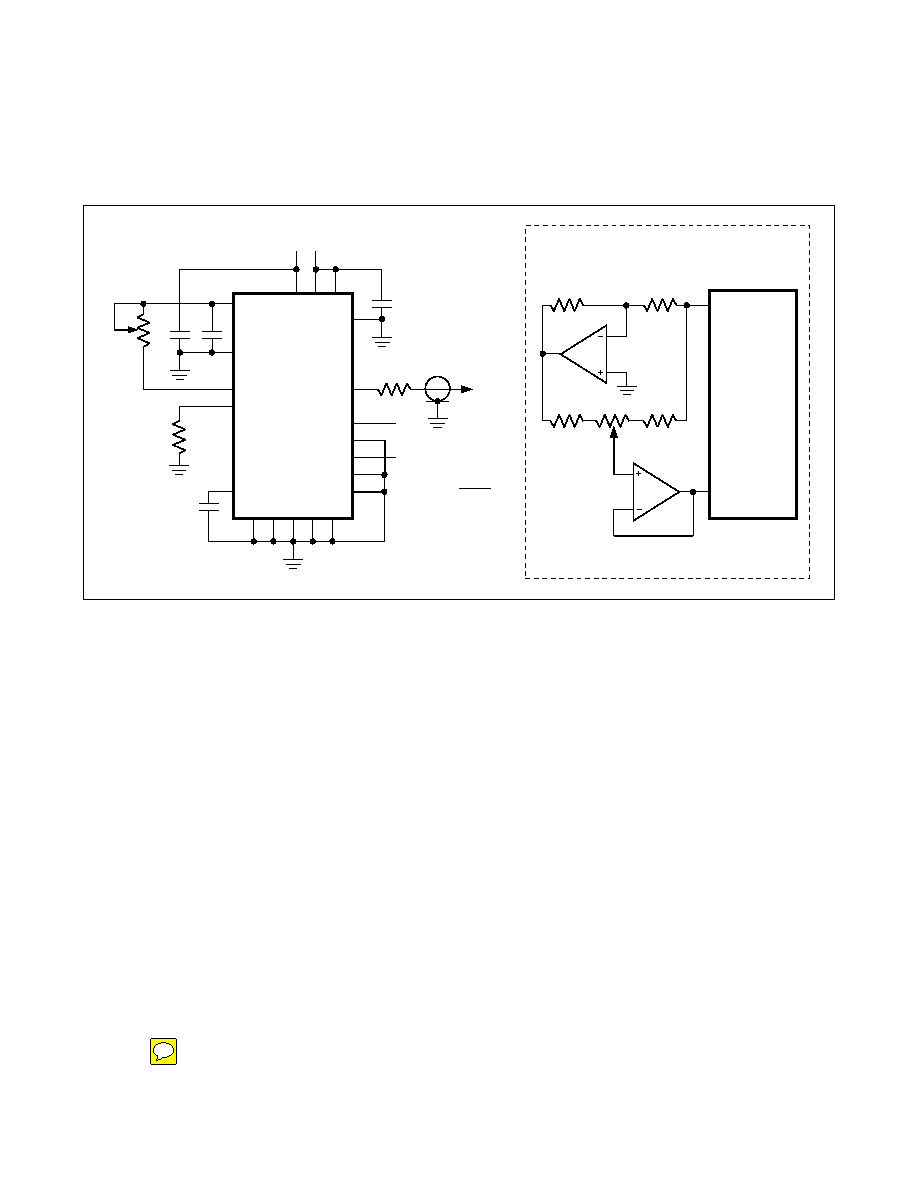
High-Frequency Waveform Generator
MAX038
1
μF
GND
COSC
12
AO
V-
18
11
9
2
6
GND GND
5
8
10
7
1
13
14
15
16
N.C.
3
FADJ
IIN
DADJ
REF
OUT
DV+
DGND
SYNC
PDI
PDO
V+ A1
4
17
20
–5V +5V
C2
1nF
C3
1
μF
C1
12k
Ω
R1
20k
Ω
RIN
FREQUENCY
50
Ω
R2
N.C.
CF
19
SINE-WAVE
OUTPUT
2 x 2.5V
RIN x CF
Fo =
MAX038
100k
Ω
R5
5k
Ω
R6
100k
Ω
R7
100k
Ω
R3
100k
Ω
R4
DADJ
REF
+2.5V
–2.5V
PRECISION DUTY-CYCLE ADJUSTMENT CIRCUIT
ADJUST R6 FOR MINIMUM SINE-WAVE DISTORTION
Figure 2. Operating Circuit with Sine-Wave Output and 50% Duty Cycle; SYNC and FADJ Disabled
MAX038
Maxim Integrated
11
相关PDF资料 |
PDF描述 |
|---|---|
| MAX1002CAX+T | IC ADC 6BIT 60MSPS DUAL 36-SSOP |
| MAX1003CAX | IC ADC DUAL 6-BIT 90MSPS 36-SSOP |
| MAX1011CEG+ | IC ADC 6BIT 90MSPS 24-QSOP |
| MAX105ECS+T | IC ADC 6BIT 800MSPS DL 80TQFP |
| MAX1063AEEG+ | IC ADC 10BIT 250KSPS 24-QSOP |
相关代理商/技术参数 |
参数描述 |
|---|---|
| MAX038CWP+ | 功能描述:时钟发生器及支持产品 RoHS:否 制造商:Silicon Labs 类型:Clock Generators 最大输入频率:14.318 MHz 最大输出频率:166 MHz 输出端数量:16 占空比 - 最大:55 % 工作电源电压:3.3 V 工作电源电流:1 mA 最大工作温度:+ 85 C 安装风格:SMD/SMT 封装 / 箱体:QFN-56 |
| MAX038CWP+T | 功能描述:时钟发生器及支持产品 RoHS:否 制造商:Silicon Labs 类型:Clock Generators 最大输入频率:14.318 MHz 最大输出频率:166 MHz 输出端数量:16 占空比 - 最大:55 % 工作电源电压:3.3 V 工作电源电流:1 mA 最大工作温度:+ 85 C 安装风格:SMD/SMT 封装 / 箱体:QFN-56 |
| MAX038CWP-T | 功能描述:时钟发生器及支持产品 RoHS:否 制造商:Silicon Labs 类型:Clock Generators 最大输入频率:14.318 MHz 最大输出频率:166 MHz 输出端数量:16 占空比 - 最大:55 % 工作电源电压:3.3 V 工作电源电流:1 mA 最大工作温度:+ 85 C 安装风格:SMD/SMT 封装 / 箱体:QFN-56 |
| MAX038EPP | 制造商:MAXIM 制造商全称:Maxim Integrated Products 功能描述:High-Frequency Waveform Generator |
| MAX038EVKIT | 制造商:MAXIM 制造商全称:Maxim Integrated Products 功能描述:Evaluation Kit for the MAX038 |
发布紧急采购,3分钟左右您将得到回复。