- 您现在的位置:买卖IC网 > PDF目录2007 > MAX1011CEG+ (Maxim Integrated Products)IC ADC 6BIT 90MSPS 24-QSOP PDF资料下载
参数资料
| 型号: | MAX1011CEG+ |
| 厂商: | Maxim Integrated Products |
| 文件页数: | 8/12页 |
| 文件大小: | 0K |
| 描述: | IC ADC 6BIT 90MSPS 24-QSOP |
| 产品培训模块: | Lead (SnPb) Finish for COTS Obsolescence Mitigation Program |
| 标准包装: | 50 |
| 位数: | 6 |
| 采样率(每秒): | 90M |
| 数据接口: | 并联 |
| 转换器数目: | 1 |
| 功率耗散(最大): | 215mW |
| 电压电源: | 单电源 |
| 工作温度: | 0°C ~ 70°C |
| 安装类型: | 表面贴装 |
| 封装/外壳: | 24-SSOP(0.154",3.90mm 宽) |
| 供应商设备封装: | 24-QSOP |
| 包装: | 管件 |
| 输入数目和类型: | 4 个单端,单极;2 个差分,单极 |
_______________Detailed Description
Converter Operation
The MAX1011 integrates a 6-bit analog-to-digital con-
verter (ADC), a buffered voltage reference, and oscilla-
tor circuitry. The ADC uses a flash conversion technique
to convert an analog input signal into a 6-bit parallel
digital output code. The MAX1011’s unique design
includes 63 fully differential comparators and a propri-
etary encoding scheme that ensures no more than
1LSB dynamic encoding error. The control logic inter-
faces easily to most digital signal processors (DSPs)
and microprocessors (Ps) with +3.3V CMOS-compati-
ble logic interfaces. Figure 1 shows the MAX1011 in a
typical application.
Programmable Input Amplifier
The MAX1011 has a programmable-gain input amplifier
with a -0.5dB bandwidth of 55MHz and a true differen-
tial input. To maximize performance in high-speed
systems, the amplifier has less than 3pF of input
capacitance. The input amplifier gain is programmed
via the GAIN pin to provide three possible input full-
scale ranges (FSRs) as shown in Table 1.
Single-ended and differential AC-coupled input circuit
examples are shown in Figures 2 and 3. Each of the
MAX1011
Low-Power, 90Msps, 6-Bit ADC
_______________________________________________________________________________________
5
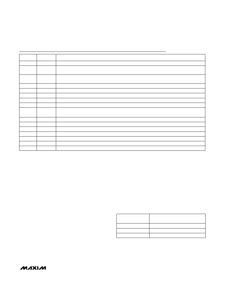
Pin Description
PIN
Gain-Select Input. Sets input full-scale range: 125/250/500mVp-p (Table 1).
GAIN
1
FUNCTION
NAME
Positive Offset-Correction Compensation. Connect a 0.22F capacitor for AC-coupled inputs. Ground
pin 2 for DC-coupled inputs.
OCC+
2
Noninverting Analog Input
IN+
4
Negative Offset-Correction Compensation. Connect a 0.22F capacitor for AC-coupled inputs. Ground
pin 3 for DC-coupled inputs.
OCC-
3
+5V ±5% Supply. Bypass with a 0.01F capacitor to GND (pin 9).
VCC
6
Analog Ground
GND
9, 10,
12, 13
Inverting Analog Input
IN-
5
+5V ±5% Supply. Bypass with a 0.01F capacitor to GND (pin 10).
VCC
11
Digital Clock Output. Frames the output data.
DCLK
18
Digital Output Supply, +3.3V ±300mV. Bypass with a 47pF capacitor to OGND (pin 16).
VCCO
17
Digital Outputs 0–5. D5 is the most significant bit (MSB).
D0–D5
19–24
250
Open
125
VCC
GAIN
500
GND
INPUT FULL-SCALE RANGE
(mVp-p)
Table 1. Input Amplifier Programming
Positive Oscillator/Clock Input
TNK+
7
Negative Oscillator/Clock Input
TNK-
8
No Connection
N.C.
15
Digital Output Ground
OGND
16
+5V ±5% Supply. Bypass with a 0.01F capacitor to GND (pin 13).
VCC
14
相关PDF资料 |
PDF描述 |
|---|---|
| MAX105ECS+T | IC ADC 6BIT 800MSPS DL 80TQFP |
| MAX1063AEEG+ | IC ADC 10BIT 250KSPS 24-QSOP |
| MAX107ECS+ | IC ADC 6BIT 400MSPS DL 80-TQFP |
| MAX1080AEUP+ | IC ADC 10BIT 400KSPS 20-TSSOP |
| MAX1084AESA+ | IC ADC 10BIT 400KSPS 8-SOIC |
相关代理商/技术参数 |
参数描述 |
|---|---|
| MAX1011CEG+ | 功能描述:模数转换器 - ADC Low-Power 90Msps 6-Bit RoHS:否 制造商:Texas Instruments 通道数量:2 结构:Sigma-Delta 转换速率:125 SPs to 8 KSPs 分辨率:24 bit 输入类型:Differential 信噪比:107 dB 接口类型:SPI 工作电源电压:1.7 V to 3.6 V, 2.7 V to 5.25 V 最大工作温度:+ 85 C 安装风格:SMD/SMT 封装 / 箱体:VQFN-32 |
| MAX1011CEG+T | 功能描述:模数转换器 - ADC Low-Power 90Msps 6-Bit RoHS:否 制造商:Texas Instruments 通道数量:2 结构:Sigma-Delta 转换速率:125 SPs to 8 KSPs 分辨率:24 bit 输入类型:Differential 信噪比:107 dB 接口类型:SPI 工作电源电压:1.7 V to 3.6 V, 2.7 V to 5.25 V 最大工作温度:+ 85 C 安装风格:SMD/SMT 封装 / 箱体:VQFN-32 |
| MAX1011CEG-T | 功能描述:模数转换器 - ADC RoHS:否 制造商:Texas Instruments 通道数量:2 结构:Sigma-Delta 转换速率:125 SPs to 8 KSPs 分辨率:24 bit 输入类型:Differential 信噪比:107 dB 接口类型:SPI 工作电源电压:1.7 V to 3.6 V, 2.7 V to 5.25 V 最大工作温度:+ 85 C 安装风格:SMD/SMT 封装 / 箱体:VQFN-32 |
| MAX1011EVKIT | 功能描述:数据转换 IC 开发工具 RoHS:否 制造商:Texas Instruments 产品:Demonstration Kits 类型:ADC 工具用于评估:ADS130E08 接口类型:SPI 工作电源电压:- 6 V to + 6 V |
| MAX101A | 制造商:MAXIM 制造商全称:Maxim Integrated Products 功能描述:500Msps, 8-Bit ADC with Track/Hold |
发布紧急采购,3分钟左右您将得到回复。