- 您现在的位置:买卖IC网 > PDF目录9469 > MAX1048BETX+T (Maxim Integrated Products)IC ADC/DAC 10BIT 36-TQFN-EP PDF资料下载
参数资料
| 型号: | MAX1048BETX+T |
| 厂商: | Maxim Integrated Products |
| 文件页数: | 8/39页 |
| 文件大小: | 0K |
| 描述: | IC ADC/DAC 10BIT 36-TQFN-EP |
| 产品培训模块: | Lead (SnPb) Finish for COTS Obsolescence Mitigation Program |
| 标准包装: | 2,500 |
| 类型: | ADC,DAC |
| 分辨率(位): | 10 b |
| 采样率(每秒): | 225k |
| 数据接口: | 串行 |
| 电压电源: | 模拟和数字 |
| 电源电压: | 4.75 V ~ 5.25 V |
| 工作温度: | -40°C ~ 85°C |
| 安装类型: | 表面贴装 |
| 封装/外壳: | 36-WFQFN 裸露焊盘 |
| 供应商设备封装: | 36-TQFN 裸露焊盘(6x6) |
| 包装: | 带卷 (TR) |
第1页第2页第3页第4页第5页第6页第7页当前第8页第9页第10页第11页第12页第13页第14页第15页第16页第17页第18页第19页第20页第21页第22页第23页第24页第25页第26页第27页第28页第29页第30页第31页第32页第33页第34页第35页第36页第37页第38页第39页
MAX1040/MAX1042/MAX1046/MAX1048
10-Bit, Multichannel ADCs/DACs with FIFO,
Temperature Sensing, and GPIO Ports
16
______________________________________________________________________________________
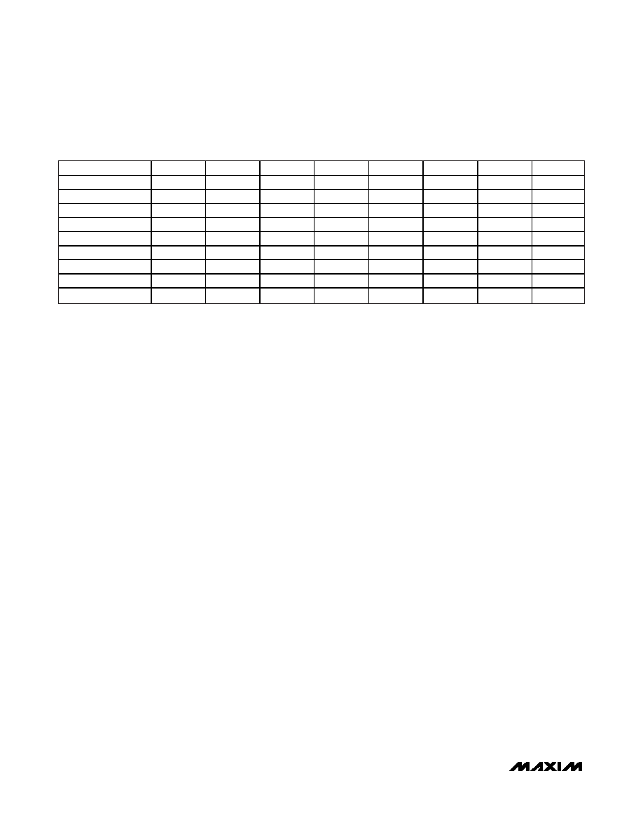
Table 1. Command Byte (MSB First)
REGISTER NAME
BIT 7
BIT 6
BIT 5
BIT 4
BIT 3
BIT 2
BIT 1
BIT 0
Conversion*
1
X
CHSEL2
CHSEL1
CHSEL0
SCAN1
SCAN0
TEMP
Setup
0
1
CKSEL1
CKSEL0
REFSEL1
REFSEL0
DIFFSEL1
DIFFSEL0
ADC Averaging
0
1
AVGON
NAVG1
NAVG0
NSCAN1
NSCAN0
DAC Select
0
1
XXXX
Reset
0
1
RESET
SLOW
FBGON
GPIO Configure**
0
000011
GPIO Write**
00
000010
GPIO Read**
0
000001
No Operation
0
000000
X = Don’t care.
*
CHESL2 bit is only valid on the MAX1040/MAX1042. Set CHSEL2 to 0 on the MAX1046/MAX1048.
**
Only applicable on the MAX1042/MAX1048.
Power-Up Default State
The MAX1040/MAX1042/MAX1046/MAX1048 power up
with all blocks in shutdown (including the reference). All
registers power up in state 00000000, except for the
setup register and the DAC input register. The setup
register powers up at 0010 1000 with CKSEL1 = 1 and
REFSEL1 = 1. The DAC input register powers up to
FFFh when RES_SEL is high, and it powers up to 000h
when RES_SEL is low.
10-Bit ADC
The MAX1040/MAX1042/MAX1046/MAX1048 ADCs use
a fully differential successive-approximation register
(SAR) conversion technique and on-chip track-and-
hold (T/H) circuitry to convert temperature and voltage
signals into 10-bit digital results. The analog inputs
accept both single-ended and differential input signals.
Single-ended signals are converted using a unipolar
transfer function, and differential signals are converted
using a selectable bipolar or unipolar transfer function.
See the
ADC Transfer Functions section for more data.
ADC Clock Modes
When addressing the setup, register bits 5 and 4 of the
command byte (CKSEL1 and CKSEL0, respectively)
control the ADC clock modes. See Table 5. Choose
between four different clock modes for various ways to
start a conversion and determine whether the acquisi-
tions are internally or externally timed. Select clock
mode 00 to configure
CNVST/AIN_ to act as a conver-
sion start and use it to request internally timed conver-
sions, without tying up the serial bus. In clock mode 01,
use
CNVST to request conversions one channel at a
time, thereby controlling the sampling speed without
tying up the serial bus. Request and start internally
timed conversions through the serial interface by writ-
ing to the conversion register in the default clock mode,
10. Use clock mode 11 with SCLK up to 3.6MHz for
externally timed acquisitions to achieve sampling rates
up to 225ksps. Clock mode 11 disables scanning and
averaging. See Figures 6–9 for timing specifications on
how to begin a conversion.
These devices feature an active-low, end-of-conversion
output.
EOC goes low when the ADC completes the last
requested operation and is waiting for the next com-
mand byte.
EOC goes high when CS or CNVST go low.
EOC is always high in clock mode 11.
Single-Ended or Differential Conversions
The MAX1040/MAX1042/MAX1046/MAX1048 use a fully
differential ADC for all conversions. When a pair of
inputs are connected as a differential pair, each input is
connected to the ADC. When configured in single-
ended mode, the positive input is the single-ended
channel and the negative input is referred to AGND.
See Figure 2.
In differential mode, the T/H samples the difference
between two analog inputs, eliminating common-mode
DC offsets and noise. IN+ and IN- are selected from the
following pairs: AIN0/AIN1, AIN2/AIN3, AIN4/AIN5,
AIN6/AIN7. AIN0–AIN3 are available on all devices.
AIN0–AIN7 are available on the MAX1040/MAX1042.
See Tables 5–8 for more details on configuring the
inputs. For the inputs that are configurable as
CNVST,
REF2, and an analog input, only one function can be
used at a time.
相关PDF资料 |
PDF描述 |
|---|---|
| MAX192BCWP+T | IC ADC 10BIT SERIAL 20-SOIC |
| V300A5M300BG3 | CONVERTER MOD DC/DC 5V 300W |
| LTC6900CS5#TRPBF | IC OSC SILICON 20MHZ TSOT23-5 |
| LTC6900CS5#TRM | IC OSC SILICON 20MHZ TSOT23-5 |
| CS5372A-ISZR | IC MODULATOR LP/HP 2CH 24-SSOP |
相关代理商/技术参数 |
参数描述 |
|---|---|
| MAX1049 | 制造商:MAXIM 制造商全称:Maxim Integrated Products 功能描述:10-Bit, Multichannel ADCs/DACs with FIFO, Temperature Sensing, and GPIO Ports |
| MAX104CHC | 制造商:Maxim from Components Direct 功能描述:MAX104CHC ANALOG TO DIGITAL CONVERTERS (ADC) - Trays 制造商:Maxim 功能描述:Maxim Integrated Products MAX104CHC Analog to Digital Converters (ADC) |
| MAX104CHC-D | 制造商:Maxim Integrated Products 功能描述:ADC SGL FLASH 1GSPS 8BIT PARALLEL 192PIN ESBGA - Trays |
| MAX104CHC-TD | 制造商:Maxim Integrated Products 功能描述:ADC SGL FLASH 1GSPS 8BIT PARALLEL 192PIN ESBGA - Tape and Reel |
| MAX104EVKIT | 制造商:Maxim Integrated Products 功能描述:KIT PKG - Bulk |
发布紧急采购,3分钟左右您将得到回复。