- 您现在的位置:买卖IC网 > PDF目录2085 > MAX1069BEUD+ (Maxim Integrated Products)IC ADC 14BIT I2C 58KSPS 14-TSSOP PDF资料下载
参数资料
| 型号: | MAX1069BEUD+ |
| 厂商: | Maxim Integrated Products |
| 文件页数: | 10/20页 |
| 文件大小: | 0K |
| 描述: | IC ADC 14BIT I2C 58KSPS 14-TSSOP |
| 标准包装: | 96 |
| 位数: | 14 |
| 采样率(每秒): | 58k |
| 数据接口: | 串行 |
| 转换器数目: | 1 |
| 功率耗散(最大): | 12.5mW |
| 电压电源: | 单电源 |
| 工作温度: | -40°C ~ 85°C |
| 安装类型: | 表面贴装 |
| 封装/外壳: | 14-TSSOP(0.173",4.40mm 宽) |
| 供应商设备封装: | 14-TSSOP |
| 包装: | 管件 |
| 输入数目和类型: | 1 个单端,单极 |
MAX1069
after a conversion. This allows more time for the input
buffer amplifier to respond to a large step-change in
input signal. The input amplifier must have a high
enough slew rate to complete the required output volt-
age change before the beginning of the acquisition
time. At the beginning of acquisition, the internal sam-
pling capacitor array connects to AIN (the amplifier out-
put), causing some output disturbance.
Ensure that the sampled voltage has settled to within
the required limits before the end of the acquisition
time. If the frequency of interest is low, AIN can be
bypassed with a large enough capacitor to charge the
internal sampling capacitor with very little ripple.
However, for AC use, AIN must be driven by a wide-
band buffer (at least 4MHz), which must be stable with
the ADC’s capacitive load (in parallel with any AIN
bypass capacitor used) and also settle quickly. Refer to
Maxim’s website at www.maxim-ic.com for application
notes on how to choose the optimum buffer amplifier for
your ADC application.
Layout, Grounding, and Bypassing
Careful printed circuit (PC) layout is essential for the
best system performance. Boards should have sepa-
rate analog and digital ground planes and ensure that
digital and analog signals are separated from each
other. Do not run analog and digital (especially clock)
lines parallel to one another, or digital lines underneath
the device package.
Figure 4 shows the recommended system ground con-
nections. Establish an analog ground point at AGND
and a digital ground point at DGND. Connect all analog
grounds to the star analog ground. Connect the digital
grounds to the star digital ground. Connect the digital
ground plane to the analog ground plane at one point.
For lowest-noise operation, make the ground return to
the star ground’s power-supply low impedance and
make it as short as possible.
High-frequency noise in the AVDD power supply
degrades the ADC’s high-speed comparator perfor-
mance. Bypass AVDD to AGND with a 0.1F ceramic
surface-mount capacitor. Make bypass capacitor con-
nections as short as possible. If the power supply is
very noisy, connect a 10
resistor in series with AVDD
and a 4.7F capacitor from AVDD to AGND to create a
lowpass RC filter.
Definitions
Integral Nonlinearity
Integral nonlinearity (INL) is the deviation of the values
on an actual transfer function from a straight line. This
straight line can be either a best-straight-line fit or a line
drawn between the end points of the transfer function
once offset and gain errors have been nullified. The
MAX1069 INL is measured using the endpoint method.
Differential Nonlinearity
Differential nonlinearity (DNL) is the difference between
an actual step width and the ideal value of 1LSB. A
DNL error specification of less than 1LSB guarantees
no missing codes and a monotonic transfer function.
Aperture Jitter
Aperture jitter (tAJ) is the sample-to-sample variation in
the time between the samples (Figure 11).
Aperture Delay
Aperture delay (tAD) is the time from the falling edge of
SCL to the instant when an actual sample is taken
(Figure 11).
Signal-to-Noise Ratio
For a waveform perfectly reconstructed from digital sam-
ples, signal-to-noise ratio (SNR) is the ratio of full-scale
analog input (RMS value) to the RMS quantization error
(residual error). The ideal, theoretical minimum analog-
to-digital noise is caused by quantization error only and
results directly from the ADC’s resolution (N bits):
SNR = ((6.02 N) + 1.76)dB
In reality, noise sources besides quantization noise
exist, including thermal noise, reference noise, clock jit-
ter, etc. Therefore, SNR is computed by taking the ratio
of the RMS signal to the RMS noise, which includes all
spectral components minus the fundamental, the first
five harmonics, and the DC offset.
58.6ksps, 14-Bit, 2-Wire Serial ADC
in a 14-Pin TSSOP
18
______________________________________________________________________________________
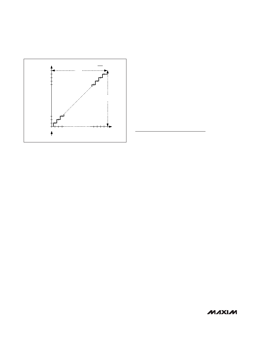
Figure 14. Unipolar Transfer Function
AGNDS
INPUT VOLTAGE (LSB)
BINAR
Y
OUTPUT
CODE
(LSB)
01 2 3
16384
1LSB =
VREF
16383
16381
0...000
0...001
0...010
0...011
1...111
1...110
1...101
1...100
VREF
V
REF
相关PDF资料 |
PDF描述 |
|---|---|
| MAX1070CTC+T | IC ADC 10BIT 1.5MSPS 12-TQFN |
| MAX1075CTC+T | IC ADC 10BIT 1.8MSPS 12-TQFN |
| MAX1078CTC+T | IC ADC 10BIT 1.8MSPS 12-TQFN |
| MAX1079CTC+T | IC ADC 10BIT 1.5MSPS 12-TQFN |
| MAX1083AEUE+ | IC ADC 10BIT 300KSPS 16-TSSOP |
相关代理商/技术参数 |
参数描述 |
|---|---|
| MAX1069BEUD+ | 功能描述:模数转换器 - ADC 58.6ksps 14-Bit 2-Wire Serial RoHS:否 制造商:Texas Instruments 通道数量:2 结构:Sigma-Delta 转换速率:125 SPs to 8 KSPs 分辨率:24 bit 输入类型:Differential 信噪比:107 dB 接口类型:SPI 工作电源电压:1.7 V to 3.6 V, 2.7 V to 5.25 V 最大工作温度:+ 85 C 安装风格:SMD/SMT 封装 / 箱体:VQFN-32 |
| MAX1069BEUD+T | 功能描述:模数转换器 - ADC 58.6ksps 14-Bit 2-Wire Serial RoHS:否 制造商:Texas Instruments 通道数量:2 结构:Sigma-Delta 转换速率:125 SPs to 8 KSPs 分辨率:24 bit 输入类型:Differential 信噪比:107 dB 接口类型:SPI 工作电源电压:1.7 V to 3.6 V, 2.7 V to 5.25 V 最大工作温度:+ 85 C 安装风格:SMD/SMT 封装 / 箱体:VQFN-32 |
| MAX1069BEUD-T | 功能描述:模数转换器 - ADC RoHS:否 制造商:Texas Instruments 通道数量:2 结构:Sigma-Delta 转换速率:125 SPs to 8 KSPs 分辨率:24 bit 输入类型:Differential 信噪比:107 dB 接口类型:SPI 工作电源电压:1.7 V to 3.6 V, 2.7 V to 5.25 V 最大工作温度:+ 85 C 安装风格:SMD/SMT 封装 / 箱体:VQFN-32 |
| MAX1069CCUD | 功能描述:模数转换器 - ADC RoHS:否 制造商:Texas Instruments 通道数量:2 结构:Sigma-Delta 转换速率:125 SPs to 8 KSPs 分辨率:24 bit 输入类型:Differential 信噪比:107 dB 接口类型:SPI 工作电源电压:1.7 V to 3.6 V, 2.7 V to 5.25 V 最大工作温度:+ 85 C 安装风格:SMD/SMT 封装 / 箱体:VQFN-32 |
| MAX1069CCUD+ | 功能描述:模数转换器 - ADC Integrated Circuits (ICs) RoHS:否 制造商:Texas Instruments 通道数量:2 结构:Sigma-Delta 转换速率:125 SPs to 8 KSPs 分辨率:24 bit 输入类型:Differential 信噪比:107 dB 接口类型:SPI 工作电源电压:1.7 V to 3.6 V, 2.7 V to 5.25 V 最大工作温度:+ 85 C 安装风格:SMD/SMT 封装 / 箱体:VQFN-32 |
发布紧急采购,3分钟左右您将得到回复。