参数资料
| 型号: | MAX1104EUA+ |
| 厂商: | Maxim Integrated Products |
| 文件页数: | 17/17页 |
| 文件大小: | 0K |
| 描述: | IC CODEC 8BIT 8-UMAX |
| 标准包装: | 50 |
| 类型: | 通用 |
| 数据接口: | * |
| 分辨率(位): | 8 b |
| ADC / DAC 数量: | 1 / 1 |
| 三角积分调变: | 无 |
| 动态范围,标准 ADC / DAC (db): | 59 / 55 |
| 电压 - 电源,模拟: | 2.7 V ~ 5.5 V |
| 电压 - 电源,数字: | 2.7 V ~ 5.5 V |
| 工作温度: | -40°C ~ 85°C |
| 安装类型: | 表面贴装 |
| 封装/外壳: | 8-TSSOP,8-MSOP(0.118",3.00mm 宽) |
| 供应商设备封装: | 8-uMAX |
| 包装: | 管件 |
LSB of the control word. Successive conversions are
initiated after the last bit of the previous conversion
result has been clocked out. Resultant data is only
available after conversion is complete.
The time required for the T/H to acquire an input signal
is a function of how quickly its input capacitance is
charged. If the input signal’s source impedance is high,
the acquisition time lengthens, and more time must be
allowed between conversions. This time, tACQ2, is cal-
culated by the following equation:
tACQ2 = (6.2 RS 15pF) + tACQ
where RS = the source impedance of the input signal;
tACQ is the T/H acquisition time from the Electrical
Characteristics table.
Conversion Progress
The comparator’s negative input is connected to the
auto-zero rail. Since the device requires only a single
supply, the ZERO node at the input of the comparator
equals VDD/2. The capacitive DAC restores node ZERO
to have no voltage difference at the comparator inputs
within the limits of an 8-bit resolution.
Input Voltage Range
Internal protection diodes that clamp the analog input
to VDD and GND allow AIN to swing from (VGND - 0.3V)
to (VDD + 0.3V) without damaging the device.
However, for accurate conversions, the input must not
exceed (VDD + 0.05V) or be less than (VGND - 0.05V).
The valid input range for the analog input is from GND
to VREF. The output code is invalid (code zero) when a
negative input voltage is applied, and full scale (FS)
when the input voltage exceeds the reference.
Input Bandwidth
The ADC’s input tracking circuitry has a 2.5MHz full-
power bandwidth, so it is possible to digitize high-
speed transient events and measure periodic signals
with bandwidths exceeding the ADC’s sampling rate by
using undersampling techniques. To avoid high-fre-
quency signals being aliased into the frequency band
of interest, low-pass filters such as the MAX7418–
MAX7426 are recommended.
Digital-to-Analog Converter
The MAX1102/MAX1103/MAX1104 DAC section uses
an R-2R ladder network that converts the 8-bit digital
input into an equivalent analog output voltage propor-
tional to the applied reference voltage (Figure 3). The
DAC features a double-buffered input, and a buffered
analog output.
MAX1102/MAX1103/MAX1104
8-Bit CODECs
_______________________________________________________________________________________
9
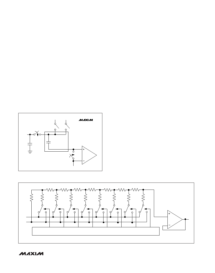
AIN
HOLD
TRACK
5pF
TRACK
ZERO
CAPACITIVE
DAC
VDD/2
VREF
GND
15pF
MAX1102
MAX1103
MAX1104
2R
R
2R
REF
GND
NOTE: SWITCH POSITIONS SHOWN FOR DAC CODE FFhex.
DAC_ REGISTER
OUT
MSB
LSB
2R
R
2R
Figure 2. Equivalent Input Circuit
Figure 3. DAC Simplified Circuit Diagram
相关PDF资料 |
PDF描述 |
|---|---|
| MAX11100EUB+ | IC ADC 16BIT SRL 200KSPS 10UMAX |
| MAX11101EUB+ | IC ADC 14BIT SRL 200KSPS 10UMAX |
| MAX11102AUB+ | IC ADC 12BIT SPI/SRL 10UMAX-EP |
| MAX1111CPE+ | IC ADC 8BIT LP 16-DIP |
| MAX1113CPE+ | IC ADC 8BIT LP 16-DIP |
相关代理商/技术参数 |
参数描述 |
|---|---|
| MAX1104EUA+ | 功能描述:ADC / DAC多通道 8-Bit CODEC RoHS:否 制造商:Texas Instruments 转换速率: 分辨率:8 bit 接口类型:SPI 电压参考: 电源电压-最大:3.6 V 电源电压-最小:2 V 最大工作温度:+ 85 C 安装风格:SMD/SMT 封装 / 箱体:VQFN-40 |
| MAX1104EUA+T | 功能描述:ADC / DAC多通道 8-Bit CODEC RoHS:否 制造商:Texas Instruments 转换速率: 分辨率:8 bit 接口类型:SPI 电压参考: 电源电压-最大:3.6 V 电源电压-最小:2 V 最大工作温度:+ 85 C 安装风格:SMD/SMT 封装 / 箱体:VQFN-40 |
| MAX1104EUA+TW | 功能描述:ADC / DAC多通道 8-Bit CODEC +2.7V to +5.5V Single Supply RoHS:否 制造商:Texas Instruments 转换速率: 分辨率:8 bit 接口类型:SPI 电压参考: 电源电压-最大:3.6 V 电源电压-最小:2 V 最大工作温度:+ 85 C 安装风格:SMD/SMT 封装 / 箱体:VQFN-40 |
| MAX1104EUA+W | 功能描述:ADC / DAC多通道 8-Bit CODEC +2.7V to +5.5V Single Supply RoHS:否 制造商:Texas Instruments 转换速率: 分辨率:8 bit 接口类型:SPI 电压参考: 电源电压-最大:3.6 V 电源电压-最小:2 V 最大工作温度:+ 85 C 安装风格:SMD/SMT 封装 / 箱体:VQFN-40 |
| MAX11054 | 制造商:MAXIM 制造商全称:Maxim Integrated Products 功能描述:4-/6-/8-Channel, 16-/14-Bit, Simultaneous-Sampling ADCs |
发布紧急采购,3分钟左右您将得到回复。