参数资料
| 型号: | MAX1104EUA+ |
| 厂商: | Maxim Integrated Products |
| 文件页数: | 3/17页 |
| 文件大小: | 0K |
| 描述: | IC CODEC 8BIT 8-UMAX |
| 标准包装: | 50 |
| 类型: | 通用 |
| 数据接口: | * |
| 分辨率(位): | 8 b |
| ADC / DAC 数量: | 1 / 1 |
| 三角积分调变: | 无 |
| 动态范围,标准 ADC / DAC (db): | 59 / 55 |
| 电压 - 电源,模拟: | 2.7 V ~ 5.5 V |
| 电压 - 电源,数字: | 2.7 V ~ 5.5 V |
| 工作温度: | -40°C ~ 85°C |
| 安装类型: | 表面贴装 |
| 封装/外壳: | 8-TSSOP,8-MSOP(0.118",3.00mm 宽) |
| 供应商设备封装: | 8-uMAX |
| 包装: | 管件 |
Serial Interface and Control Logic
The MAX1102/MAX1103/MAX1104 have 4-wire serial
interfaces (Figure 4). The CS, SCLK, and DIN inputs
are used to control and configure the device, while the
three-state DOUT provides access to the ADC conver-
sion result. DIN also serves as the data input to the
DAC.
The serial interface provides easy connection to Cs
with SPI, QSPI, and MICROWIRE serial interfaces at
clock rates up to 6MHz. For SPI and QSPI, set CPOL =
CPHA = 0 in the SPI control registers of the C. Figure
4 gives detailed timing information.
Digital Inputs and Outputs
The logic levels of the MAX1102/MAX1103/MAX1104
digital inputs are set to accept voltage levels from both
+3V and +5V systems regardless of the supply volt-
ages.
Performing a Conversion
Configuring the MAX1102/MAX1103/MAX1104
The MAX1102/MAX1103/MAX1104 must be configured
before a conversion can occur. Following CS falling, on
each rising edge of SCLK, a bit from DIN is clocked
into the MAX1102/MAX1103/MAX1104’s internal shift
register. After CS falls, the first arriving logic “1” bit
defines the MSB of the control byte (START). Until the
START bit arrives, any number of logic “0” bits can be
clocked into DIN with no effect. Table 1 shows the con-
trol-byte format.
The control word sets the mode in which the MAX1102/
MAX1103/MAX1104 operate. The enable bits, E0 to E2,
determine what sections of the device are operating by
either enabling or shutting down the two converters and
voltage reference (see
Shutdown Modes). The enable
bits are independent of the address bits; for example,
the ADC need not be addressed for it to be shutdown
or powered up.
C0 and C1 are the control bits. C0 sets the conversion
mode, either single or continuous (see
Conversion
Modes). C1 determines whether the ADC monitors
VDD/2 or AIN (see Power Sense). When changing C1,
two control words must be written. The first control
word changes the state of the mux. Then wait 3.5s for
the T/H to acquire the new input. Finally, the second
control word causes the conversion to take place. For
MAX1104 set C1 = 0.
A0 is the ADC address bit. A logic “1” on A0 addresses
the ADC. The control word configures the ADC. A logic
“0” on A0 deselects the ADC. In this state, the ADC is
still active, but does not perform any conversions.
A1 is the DAC address bit. A logic “1” on A1 address-
es the DAC. The control word configures the DAC, and
the eight bits following the control word are read in as
DAC data. The converted analog output is available
after the eighth data bit is read into the device. A logic
“0” deselects the DAC. In this state the DAC is still
active, but ignores any digital inputs.
Both the ADC and DAC can be addresses from the
same control word, allowing both converters to operate
simultaneously.
MAX1102/MAX1103/MAX1104
8-Bit CODECs
______________________________________________________________________________________
11
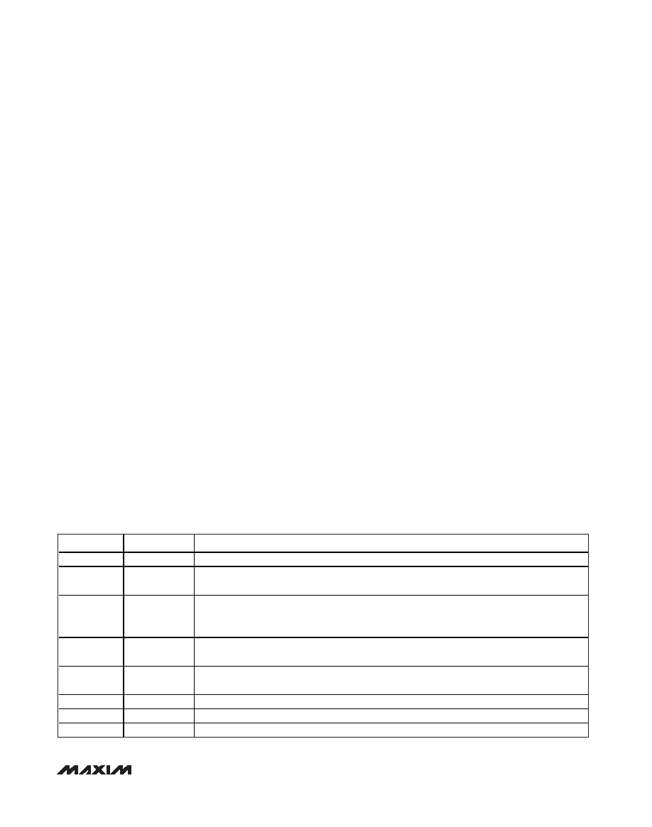
BIT
NAME
DESCRIPTION
7 (MSB)
START
1 = designates a new control word. 0 = control word ignored, unless byte is DAC data.
6A1
1 = DAC addressed. Current byte configures DAC, the following byte is DAC data.
0 = DAC not addressed.
5A0
1 = ADC addressed. Current byte configures ADC. After the 36
s conversion time, the next eight
clock cycles clock out the conversion result.
0 = ADC not addressed.
4
C1*
1 = ADC input to VDD/2.
0 = ADC input to AIN.
3C0
1 = Continuous conversion. Control word not required unless the device is reconfigured.
0 = Single conversion. New control word required before next conversion.
2
E2
1 = Reference enabled. 0 = Reference disabled. Don’t care for MAX1104.
1
E1
1 = ADC enabled. 0 = ADC disabled.
0
E0
1 = DAC enabled. 0 = DAC disabled.
Table 1. Control-Byte Format
* Leave C1 = 0 for MAX1104.
相关PDF资料 |
PDF描述 |
|---|---|
| MAX11100EUB+ | IC ADC 16BIT SRL 200KSPS 10UMAX |
| MAX11101EUB+ | IC ADC 14BIT SRL 200KSPS 10UMAX |
| MAX11102AUB+ | IC ADC 12BIT SPI/SRL 10UMAX-EP |
| MAX1111CPE+ | IC ADC 8BIT LP 16-DIP |
| MAX1113CPE+ | IC ADC 8BIT LP 16-DIP |
相关代理商/技术参数 |
参数描述 |
|---|---|
| MAX1104EUA+ | 功能描述:ADC / DAC多通道 8-Bit CODEC RoHS:否 制造商:Texas Instruments 转换速率: 分辨率:8 bit 接口类型:SPI 电压参考: 电源电压-最大:3.6 V 电源电压-最小:2 V 最大工作温度:+ 85 C 安装风格:SMD/SMT 封装 / 箱体:VQFN-40 |
| MAX1104EUA+T | 功能描述:ADC / DAC多通道 8-Bit CODEC RoHS:否 制造商:Texas Instruments 转换速率: 分辨率:8 bit 接口类型:SPI 电压参考: 电源电压-最大:3.6 V 电源电压-最小:2 V 最大工作温度:+ 85 C 安装风格:SMD/SMT 封装 / 箱体:VQFN-40 |
| MAX1104EUA+TW | 功能描述:ADC / DAC多通道 8-Bit CODEC +2.7V to +5.5V Single Supply RoHS:否 制造商:Texas Instruments 转换速率: 分辨率:8 bit 接口类型:SPI 电压参考: 电源电压-最大:3.6 V 电源电压-最小:2 V 最大工作温度:+ 85 C 安装风格:SMD/SMT 封装 / 箱体:VQFN-40 |
| MAX1104EUA+W | 功能描述:ADC / DAC多通道 8-Bit CODEC +2.7V to +5.5V Single Supply RoHS:否 制造商:Texas Instruments 转换速率: 分辨率:8 bit 接口类型:SPI 电压参考: 电源电压-最大:3.6 V 电源电压-最小:2 V 最大工作温度:+ 85 C 安装风格:SMD/SMT 封装 / 箱体:VQFN-40 |
| MAX11054 | 制造商:MAXIM 制造商全称:Maxim Integrated Products 功能描述:4-/6-/8-Channel, 16-/14-Bit, Simultaneous-Sampling ADCs |
发布紧急采购,3分钟左右您将得到回复。