参数资料
| 型号: | MAX11206EEE+T |
| 厂商: | Maxim Integrated Products |
| 文件页数: | 7/27页 |
| 文件大小: | 0K |
| 描述: | IC ADC 20BIT 16QSOP |
| 产品培训模块: | Lead (SnPb) Finish for COTS Obsolescence Mitigation Program |
| 标准包装: | 2,500 |
| 位数: | 20 |
| 采样率(每秒): | 480 |
| 数据接口: | MICROWIRE?,QSPI?,串行,SPI? |
| 转换器数目: | 1 |
| 功率耗散(最大): | 667mW |
| 电压电源: | 模拟和数字,双 ± |
| 工作温度: | -40°C ~ 85°C |
| 安装类型: | 表面贴装 |
| 封装/外壳: | 16-SSOP(0.154",3.90mm 宽) |
| 供应商设备封装: | 16-QSOP |
| 包装: | 带卷 (TR) |
| 输入数目和类型: | 1 个差分,单极;1 个差分,双极 |
第1页第2页第3页第4页第5页第6页当前第7页第8页第9页第10页第11页第12页第13页第14页第15页第16页第17页第18页第19页第20页第21页第22页第23页第24页第25页第26页第27页
15
Maxim Integrated
20-Bit, Single-Channel, Ultra-Low-Power, Delta-
Sigma ADCs with Programmable Gain and GPIO
MAX11206/MAX11207
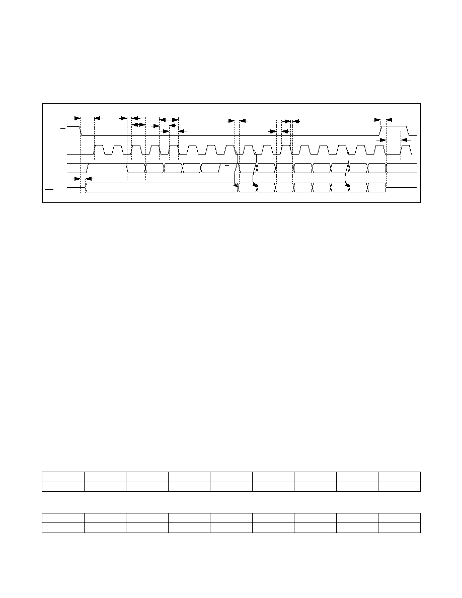
Figure 7. SPI Register Access Read
Table 5. Command Byte (MODE = 0)
Table 6. Command Byte (MODE = 1)
Note: The START bit is used to synchronize the data from the host device. The START bit is always 1.
Command Byte
Communication between the user and the device is con-
ducted through SPI using a command byte. The com-
mand byte consists of two modes differentiated as com-
mand modes and data modes. Command modes and
data modes are further differentiated by decoding the
remaining bits in the command byte. The mode selected
is determined by the MODE bit. If the MODE bit is 0, then
the user is requesting either a conversion, calibration, or
power-down; see Table 5. If the MODE bit is 1, then the
user is selecting a data command and can either read
from or write to a register; see Table 6.
The Status register (STAT1) is a read-only register and
provides general chip operational status to the user. If
the user attempts to calibrate the system and overranges
the internal signal scaling, then a gain overrange condi-
tion is flagged with the SYSOR bit. The last data rate
programmed for the ADC is available in the RATE bits.
If the input signal has exceeded positive or negative full
scale, this condition is flagged with the OR and UR bits.
If the modulator is busy converting, then the MSTAT bit
is set. If a conversion result is ready for readout, the RDY
bit is set; see Table 11.
The Control 1 register (CTRL1) is a read/write register,
and the bits determine the internal oscillator frequency,
unipolar or bipolar input range, selection of an internal or
external clock, enabling or disabling the reference and
input signal buffers, the output data format (offset binary
or two’s complement), and single-cycle or continuous
conversion mode. See Table 12.
The Control 2 register (CTRL2) is a read/write register,
and the bits configure the GPIOs as inputs or outputs
and their values. See Table 13.
The Control 3 register (CTRL3) is a read/write register,
and the bits determine the MAX11206 programmable
gain setting and the calibration register settings for both
the MAX11206 and MAX11207. See Table 14.
The Data register (DATA) is a read-only register. Data is
output from RDY/DOUT on the next 24 SCLK cycles once
CS is forced low. The data bits transition on the falling
edge of SCLK. Data is output MSB first, and is offset
binary or two’s complement, depending on the setting
of the FORMAT bit in the CTRL1 register. See Table 15.
The System Offset Calibration register (SOC) is a read/
write register, and the bits contain the digital value that
corrects the data for system zero scale. See Table 17.
The System Gain Calibration register (SGC) is a read/
write register, and the bits contain the digital value that
corrects the data for system full scale. See Table 18.
The Self-Cal Offset Calibration register (SCOC) is a read/
write register, and the bits contain the value that corrects
the data for chip zero scale. See Table 19.
The Self-Cal Gain Calibration register (SCGC) is a read/
write register, and the bits contain the value that corrects
the data for chip full scale. See Table 20.
tDOE
HIGH-Z
SCLK
X
1
11
X
RS3
RS2
RS1
RS0
W/R
XX
X
XXX
XX
D6
D7
D5
D4
D3
D2
D1
D0
16
89
DIN
tCP
tDOD
tDOT
tDO1
tDOH
CS
RDY/DOUT
tCSS0
tDS
tCSS1
tCL
tCH
tDH
BIT
B7
B6
B5
B4
B3
B2
B1
B0
BIT NAME
START = 1
MODE = 0
CAL1
CAL0
IMPD
RATE2
RATE1
RATE0
BIT
B7
B6
B5
B4
B3
B2
B1
B0
BIT NAME
START = 1
MODE = 1
0
RS3
RS2
RS1
RS0
W/R
相关PDF资料 |
PDF描述 |
|---|---|
| GTC06A-20-18P | CONN PLUG 9POS STRAIGHT W/PINS |
| IDT723634L15PF8 | IC FIFO SYNC 512X36X2 128QFP |
| MAX11626EEE+T | IC ADC 12BIT 4CH 16QSOP |
| IDT72815LB25BG8 | IC FIFO SYNC DUAL 512X18 121BGA |
| MS3101R20-27S | CONN RCPT 14POS PANEL MNT W/SCKT |
相关代理商/技术参数 |
参数描述 |
|---|---|
| MAX11206EVKIT+ | 功能描述:数据转换 IC 开发工具 20-Bit Single Channel Delta Sigma RoHS:否 制造商:Texas Instruments 产品:Demonstration Kits 类型:ADC 工具用于评估:ADS130E08 接口类型:SPI 工作电源电压:- 6 V to + 6 V |
| MAX11207 | 制造商:MAXIM 制造商全称:Maxim Integrated Products 功能描述:20-Bit, Single-Channel, Ultra-Low-Power, Delta-Sigma ADCs with Programmable Gain and GPIO |
| MAX11207EEE+ | 功能描述:模数转换器 - ADC 20-Bit Delta-Sigma RoHS:否 制造商:Texas Instruments 通道数量:2 结构:Sigma-Delta 转换速率:125 SPs to 8 KSPs 分辨率:24 bit 输入类型:Differential 信噪比:107 dB 接口类型:SPI 工作电源电压:1.7 V to 3.6 V, 2.7 V to 5.25 V 最大工作温度:+ 85 C 安装风格:SMD/SMT 封装 / 箱体:VQFN-32 |
| MAX11207EEE+T | 功能描述:模数转换器 - ADC 20-Bit Delta-Sigma RoHS:否 制造商:Texas Instruments 通道数量:2 结构:Sigma-Delta 转换速率:125 SPs to 8 KSPs 分辨率:24 bit 输入类型:Differential 信噪比:107 dB 接口类型:SPI 工作电源电压:1.7 V to 3.6 V, 2.7 V to 5.25 V 最大工作温度:+ 85 C 安装风格:SMD/SMT 封装 / 箱体:VQFN-32 |
| MAX11208 | 制造商:MAXIM 制造商全称:Maxim Integrated Products 功能描述:20-Bit, Single-Channel, Ultra-Low-Power, Delta-Sigma ADC with 2-Wire Serial Interface |
发布紧急采购,3分钟左右您将得到回复。