- 您现在的位置:买卖IC网 > PDF目录17008 > MAX11633EVKIT# (Maxim Integrated Products)KIT EVALUATION FOR MAX11633 PDF资料下载
参数资料
| 型号: | MAX11633EVKIT# |
| 厂商: | Maxim Integrated Products |
| 文件页数: | 11/22页 |
| 文件大小: | 0K |
| 描述: | KIT EVALUATION FOR MAX11633 |
| 产品培训模块: | Lead (SnPb) Finish for COTS Obsolescence Mitigation Program |
| 标准包装: | 1 |
| 系列: | * |
MAX11626–MAX11629/MAX11632/MAX11633
12-Bit, 300ksps ADCs
with FIFO and Internal Reference
______________________________________________________________________________________
19
Initiate a conversion by writing a byte to the conversion
register followed by 16 SCLK cycles. If CS is pulsed
high between the eight and ninth cycles, the pulse
width must be less than 100s. To continuously convert
at 16 cycles per conversion, alternate 1 byte of zeros
between each conversion byte.
If reference mode 00 is requested, wait 65s with CS
high after writing the conversion byte to extend the
acquisition and allow the internal reference to power up.
Partial Reads and Partial Writes
If the first byte of an entry in the FIFO is partially read
(CS is pulled high after fewer than eight SCLK cycles),
the second byte of data that is read out contains the
next 8 bits (not b7–b0). The remaining bits are lost for
that entry. If the first byte of an entry in the FIFO is read
out fully, but the second byte is read out partially, the
rest of the entry is lost. The remaining data in the FIFO
is uncorrupted and can be read out normally after tak-
ing CS low again, as long as the 4 leading bits (normal-
ly zeros) are ignored. Internal registers that are written
partially through the SPI contain new values, starting at
the MSB up to the point that the partial write is stopped.
The part of the register that is not written contains previ-
ously written values. If CS is pulled low before EOC
goes low, a conversion cannot be completed and the
FIFO is corrupted.
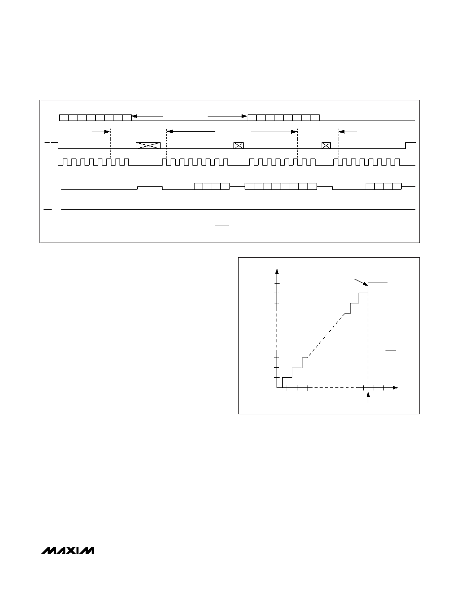
Transfer Function
Figure 8 shows the unipolar transfer function. Code tran-
sitions occur halfway between successive-integer LSB
values. Output coding is binary, with 1 LSB = VREF/2.5V
(MAX11627/MAX11629/MAX11633) and 1 LSB = VREF/
4.096V (MAX11626/MAX11628/MAX11632).
Layout, Grounding, and Bypassing
For best performance, use PCBs. Do not use wire wrap
boards. Board layout should ensure that digital and ana-
log signal lines are separated from each other. Do not
run analog and digital (especially clock) signals parallel
to one another or run digital lines underneath the
MAX11626–MAX11629/MAX11632/MAX11633 package.
High-frequency noise in the VDD power supply can
affect performance. Bypass the VDD supply with a 0.1F
capacitor to GND, close to the VDD pin. Minimize capaci-
tor lead lengths for best supply-noise rejection. If the
power supply is very noisy, connect a 10
resistor in
series with the supply to improve power-supply filtering.
CS
DOUT
SCLK
DIN
EOC
MSB1
LSB1
MSB2
(ACQUISITION1)
(ACQUISITION2)
(CONVERSION1)
(CONVERSION BYTE)
EXTERNALLY TIMED ACQUISITION, SAMPLING AND CONVERSION WITHOUT CNVST.
Figure 7. Clock Mode 11 Timing
OUTPUT CODE
FULL-SCALE
TRANSITION
11 . . .
. . . 111
11 . . .
. . . 110
11 . . .
. . . 101
00 . . .
. . . 011
00 . . .
. . . 010
00 . . .
. . . 001
00 . . .
. . . 000
12
3
0
(COM)
FS
FS - 3/2 LSB
FS = VREF + VCOM
ZS = VCOM
INPUT VOLTAGE (LSB)
1 LSB =
VREF
4096
Figure 8. Unipolar Transfer Function, Full Scale (FS) = VREF
相关PDF资料 |
PDF描述 |
|---|---|
| MAX11666EVKIT# | KIT EVAL FOR MAX11666 |
| GEM25DRYI-S13 | CONN EDGECARD 50POS .156 EXTEND |
| GCM15DRYH-S13 | CONN EDGECARD 30POS .156 EXTEND |
| VI-22X-EY | CONVERTER MOD DC/DC 5.2V 50W |
| RBM18DSXI | CONN EDGECARD 36POS DIP .156 SLD |
相关代理商/技术参数 |
参数描述 |
|---|---|
| MAX11633EVKIT# | 功能描述:数据转换 IC 开发工具 MAX11633 Eval Kit RoHS:否 制造商:Texas Instruments 产品:Demonstration Kits 类型:ADC 工具用于评估:ADS130E08 接口类型:SPI 工作电源电压:- 6 V to + 6 V |
| MAX11633EVKIT+ | 制造商:Maxim Integrated Products 功能描述:12-BIT 300KSPS ADCS 16-CHANNEL WITH FIFO AND INTERNAL REFERE - Boxed Product (Development Kits) |
| MAX11633EVSYS# | 功能描述:数据转换 IC 开发工具 MAX11633 Eval Kit RoHS:否 制造商:Texas Instruments 产品:Demonstration Kits 类型:ADC 工具用于评估:ADS130E08 接口类型:SPI 工作电源电压:- 6 V to + 6 V |
| MAX11634 | 制造商:MAXIM 制造商全称:Maxim Integrated Products 功能描述:12-Bit, 300ksps ADCs with Differential |
| MAX11634EEE+ | 功能描述:模数转换器 - ADC 12-Bit 4Ch 300ksps High Speed ADC RoHS:否 制造商:Texas Instruments 通道数量:2 结构:Sigma-Delta 转换速率:125 SPs to 8 KSPs 分辨率:24 bit 输入类型:Differential 信噪比:107 dB 接口类型:SPI 工作电源电压:1.7 V to 3.6 V, 2.7 V to 5.25 V 最大工作温度:+ 85 C 安装风格:SMD/SMT 封装 / 箱体:VQFN-32 |
发布紧急采购,3分钟左右您将得到回复。