- 您现在的位置:买卖IC网 > PDF目录17008 > MAX11633EVKIT# (Maxim Integrated Products)KIT EVALUATION FOR MAX11633 PDF资料下载
参数资料
| 型号: | MAX11633EVKIT# |
| 厂商: | Maxim Integrated Products |
| 文件页数: | 12/22页 |
| 文件大小: | 0K |
| 描述: | KIT EVALUATION FOR MAX11633 |
| 产品培训模块: | Lead (SnPb) Finish for COTS Obsolescence Mitigation Program |
| 标准包装: | 1 |
| 系列: | * |
MAX11626–MAX11629/MAX11632/MAX11633
12-Bit, 300ksps ADCs
with FIFO and Internal Reference
2
_______________________________________________________________________________________
ABSOLUTE MAXIMUM RATINGS
ELECTRICAL CHARACTERISTICS
(VDD = +2.7V to +3.6V (MAX11627/MAX11629/MAX11633); VDD = +4.75V to +5.25V (MAX11626/MAX11628/MAX11632), fSAMPLE =
300kHz, fSCLK = 4.8MHz external clock (50% duty cycle), VREF = 2.5V (MAX11627//MAX11629/MAX11633); VREF = 4.096V
(MAX11626/MAX11628/MAX11632), TA = TMIN to TMAX, unless otherwise noted. Typical values are at TA = +25°C.)
Stresses beyond those listed under “Absolute Maximum Ratings” may cause permanent damage to the device. These are stress ratings only, and functional
operation of the device at these or any other conditions beyond those indicated in the operational sections of the specifications is not implied. Exposure to
absolute maximum rating conditions for extended periods may affect device reliability.
VDD to GND ..............................................................-0.3V to +6V
CS, SCLK, DIN, EOC, DOUT to GND.........-0.3V to (VDD + 0.3V)
AIN0–AIN13, AIN_, CNVST/AIN_,
REF to GND ...........................................-0.3V to (VDD + 0.3V)
Maximum Current into Any Pin............................................50mA
Continuous Power Dissipation (TA = +70°C)
16-Pin QSOP (derate 8.3mW/°C above +70°C)...........667mW
24-Pin QSOP (derate 9.5mW/°C above +70°C)...........762mW
Operating Temperature Range ...........................-40°C to +85°C
Storage Temperature Range .............................-60°C to +150°C
Junction Temperature ......................................................+150°C
Lead Temperature (soldering, 10s) .................................+300°C
Soldering Temperature (reflow) .......................................+260°C
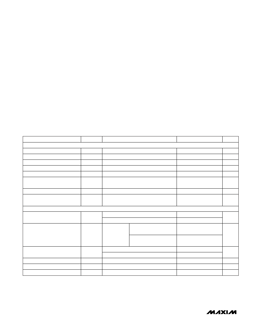
PARAMETER
SYMBOL
CONDITIONS
MIN
TYP
MAX
UNITS
DC ACCURACY (Note 1)
Resolution
RES
12
Bits
Integral Nonlinearity
INL
±1.0
LSB
Differential Nonlinearity
DNL
No missing codes over temperature
±1.0
LSB
Offset Error
±0.5
±4.0
LSB
Gain Error
(Note 2)
±0.5
±4.0
LSB
Offset Error Temperature
Coefficient
±2
ppm/°C
FSR
Gain Temperature Coefficient
±0.8
ppm/°C
Channel-to-Channel Offset
Matching
±0.1
LSB
DYNAMIC SPECIFICATIONS (30kHz sine-wave input, 300ksps, fSCLK = 4.8MHz)
MAX11627/MAX11629/MAX11633
71
Signal-to-Noise Plus Distortion
SINAD
MAX11626/MAX11628/MAX11632
73
dB
MAX11627/MAX11629/
MAX11633
-80
Total Harmonic Distortion
THD
Up to the 5th
harmonic
MAX11626/MAX11628/
MAX11632
-88
dBc
MAX11627/MAX11629/MAX11633
81
Spurious-Free Dynamic Range
SFDR
MAX11626/MAX11628/MAX11632
89
dBc
Intermodulation Distortion
IMD
fIN1 = 29.9kHz, fIN2 = 30.2kHz
76
dBc
Full-Power Bandwidth
-3dB point
1
MHz
Full-Linear Bandwidth
S/(N + D) > 68dB
100
kHz
相关PDF资料 |
PDF描述 |
|---|---|
| MAX11666EVKIT# | KIT EVAL FOR MAX11666 |
| GEM25DRYI-S13 | CONN EDGECARD 50POS .156 EXTEND |
| GCM15DRYH-S13 | CONN EDGECARD 30POS .156 EXTEND |
| VI-22X-EY | CONVERTER MOD DC/DC 5.2V 50W |
| RBM18DSXI | CONN EDGECARD 36POS DIP .156 SLD |
相关代理商/技术参数 |
参数描述 |
|---|---|
| MAX11633EVKIT# | 功能描述:数据转换 IC 开发工具 MAX11633 Eval Kit RoHS:否 制造商:Texas Instruments 产品:Demonstration Kits 类型:ADC 工具用于评估:ADS130E08 接口类型:SPI 工作电源电压:- 6 V to + 6 V |
| MAX11633EVKIT+ | 制造商:Maxim Integrated Products 功能描述:12-BIT 300KSPS ADCS 16-CHANNEL WITH FIFO AND INTERNAL REFERE - Boxed Product (Development Kits) |
| MAX11633EVSYS# | 功能描述:数据转换 IC 开发工具 MAX11633 Eval Kit RoHS:否 制造商:Texas Instruments 产品:Demonstration Kits 类型:ADC 工具用于评估:ADS130E08 接口类型:SPI 工作电源电压:- 6 V to + 6 V |
| MAX11634 | 制造商:MAXIM 制造商全称:Maxim Integrated Products 功能描述:12-Bit, 300ksps ADCs with Differential |
| MAX11634EEE+ | 功能描述:模数转换器 - ADC 12-Bit 4Ch 300ksps High Speed ADC RoHS:否 制造商:Texas Instruments 通道数量:2 结构:Sigma-Delta 转换速率:125 SPs to 8 KSPs 分辨率:24 bit 输入类型:Differential 信噪比:107 dB 接口类型:SPI 工作电源电压:1.7 V to 3.6 V, 2.7 V to 5.25 V 最大工作温度:+ 85 C 安装风格:SMD/SMT 封装 / 箱体:VQFN-32 |
发布紧急采购,3分钟左右您将得到回复。