- 您现在的位置:买卖IC网 > PDF目录17007 > MAX1231EVKIT (Maxim Integrated Products)EVAL KIT FOR MAX1231 PDF资料下载
参数资料
| 型号: | MAX1231EVKIT |
| 厂商: | Maxim Integrated Products |
| 文件页数: | 17/22页 |
| 文件大小: | 0K |
| 描述: | EVAL KIT FOR MAX1231 |
| 产品培训模块: | Lead (SnPb) Finish for COTS Obsolescence Mitigation Program |
| 标准包装: | 1 |
| ADC 的数量: | 1 |
| 位数: | 12 |
| 采样率(每秒): | 300k |
| 数据接口: | 串行 |
| 输入范围: | ±VREF/2 |
| 在以下条件下的电源(标准): | 1.86mW @ 300kSPS |
| 工作温度: | 0°C ~ 70°C |
| 已用 IC / 零件: | MAX1231 |
| 已供物品: | 板,CD |
MAX1227/MAX1229/MAX1231
12-Bit 300ksps ADCs with FIFO,
Temp Sensor, Internal Reference
4
_______________________________________________________________________________________
Note 1: Tested at VDD = +2.7V, unipolar input mode.
Note 2: Offset nulled.
Note 3: Time for reference to power up and settle to within 1 LSB.
Note 4: Conversion time is defined as the number of clock cycles multiplied by the clock period; clock has 50% duty cycle.
Note 5: The operational input voltage range for each individual input of a differentially configured pair is from GND to VDD. The
operational input voltage difference is from -VREF/2 to +VREF/2.
Note 6: See Figure 3 (Input Equivalent Circuit) and the Typical Operating Curve in the
Sampling Error vs. Source Impedance sec-
tion.
Note 7: Fast automated test, excludes self-heating effects.
Note 8: When CNVST is configured as a digital input, do not apply a voltage between VIL and VIN.
Note 9: Supply current is specified depending on whether an internal or external reference is used for voltage conversions.
Temperature measurements always use the internal reference.
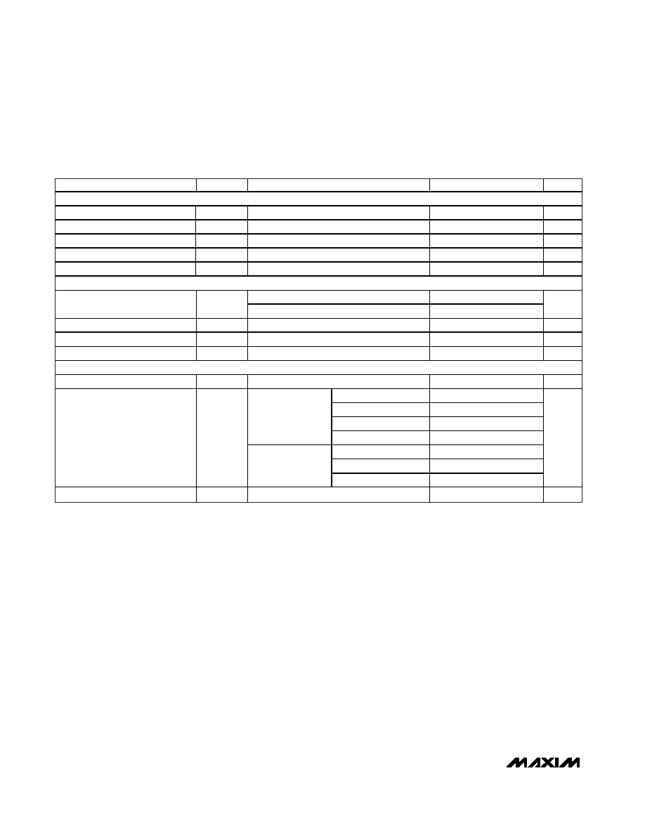
ELECTRICAL CHARACTERISTICS (continued)
(VDD = +2.7V to +3.6V, fSAMPLE = 300kHz, fSCLK = 4.8MHz (50% duty cycle), VREF = 2.5V, TA = TMIN to TMAX, unless otherwise
noted. Typical values are at TA = +25°C.)
PARAMETER
SYMBOL
CONDITIONS
MIN
TYP
MAX
UNITS
DIGITAL INPUTS (SCLK, DIN,
CS, CNVST) (Note 8)
Input Voltage Low
VIL
VDD x 0.3
V
Input Voltage High
VIH
VDD x 0.7
V
Input Hysteresis
VHYST
200
mV
Input Leakage Current
IIN
VIN = 0 or VDD
±0.01
±1.0
A
Input Capacitance
CIN
15
pF
DIGITAL OUTPUTS (DOUT,
EOC)
ISINK = 2mA
0.4
Output Voltage Low
VOL
ISINK = 4mA
0.8
V
Output Voltage High
VOH
ISOURCE = 1.5mA
VDD - 0.5
V
Tri-State Leakage Current
IL
CS = VDD
±0.05
±1
A
Tri-State Output Capacitance
COUT
CS = VDD
15
pF
POWER REQUIREMENTS
Supply Voltage
VDD
2.7
3.6
V
During temp sense
2400
2700
fSAMPLE = 300ksps
1750
2000
fSAMPLE = 0, REFon
1000
1200
Internal
reference
Shutdown
0.2
5
During temp sense
1550
2000
fSAMPLE = 300ksps
1050
1200
Supply Current (Note 9)
IDD
External
reference
Shutdown
0.2
5
A
Power-Supply Rejection
PSR
VDD = 2.7V to 3.6V; full-scale input
±0.2
±1
mV
相关PDF资料 |
PDF描述 |
|---|---|
| 0210490251 | CABLE JUMPER 1.25MM .254M 18POS |
| GSM11DSEN-S13 | CONN EDGECARD 22POS .156 EXTEND |
| HW-DLN-3C | ACCY ISP CABLE 8PIN AMP 10P CONN |
| MAX11040DBEVKIT+ | KIT EVALUATION FOR MAX11040 |
| MAX1231BEVKIT# | KIT EVALUATION FOR 12BIT ADCS |
相关代理商/技术参数 |
参数描述 |
|---|---|
| MAX1232C/D | 功能描述:监控电路 RoHS:否 制造商:STMicroelectronics 监测电压数: 监测电压: 欠电压阈值: 过电压阈值: 输出类型:Active Low, Open Drain 人工复位:Resettable 监视器:No Watchdog 电池备用开关:No Backup 上电复位延迟(典型值):10 s 电源电压-最大:5.5 V 最大工作温度:+ 85 C 安装风格:SMD/SMT 封装 / 箱体:UDFN-6 封装:Reel |
| MAX1232C/D DIE | 制造商:Maxim Integrated Products 功能描述: |
| MAX1232CPA | 功能描述:监控电路 RoHS:否 制造商:STMicroelectronics 监测电压数: 监测电压: 欠电压阈值: 过电压阈值: 输出类型:Active Low, Open Drain 人工复位:Resettable 监视器:No Watchdog 电池备用开关:No Backup 上电复位延迟(典型值):10 s 电源电压-最大:5.5 V 最大工作温度:+ 85 C 安装风格:SMD/SMT 封装 / 箱体:UDFN-6 封装:Reel |
| MAX1232CPA+ | 功能描述:监控电路 MPU Monitor RoHS:否 制造商:STMicroelectronics 监测电压数: 监测电压: 欠电压阈值: 过电压阈值: 输出类型:Active Low, Open Drain 人工复位:Resettable 监视器:No Watchdog 电池备用开关:No Backup 上电复位延迟(典型值):10 s 电源电压-最大:5.5 V 最大工作温度:+ 85 C 安装风格:SMD/SMT 封装 / 箱体:UDFN-6 封装:Reel |
| MAX1232CSA | 功能描述:监控电路 RoHS:否 制造商:STMicroelectronics 监测电压数: 监测电压: 欠电压阈值: 过电压阈值: 输出类型:Active Low, Open Drain 人工复位:Resettable 监视器:No Watchdog 电池备用开关:No Backup 上电复位延迟(典型值):10 s 电源电压-最大:5.5 V 最大工作温度:+ 85 C 安装风格:SMD/SMT 封装 / 箱体:UDFN-6 封装:Reel |
发布紧急采购,3分钟左右您将得到回复。