- 您现在的位置:买卖IC网 > PDF目录383316 > MAX1246ACEE (MAXIM INTEGRATED PRODUCTS INC) +2.7V, Low-Power, 4-Channel, Serial 12-Bit ADCs in QSOP-16 PDF资料下载
参数资料
| 型号: | MAX1246ACEE |
| 厂商: | MAXIM INTEGRATED PRODUCTS INC |
| 元件分类: | ADC |
| 英文描述: | +2.7V, Low-Power, 4-Channel, Serial 12-Bit ADCs in QSOP-16 |
| 中文描述: | 4-CH 12-BIT SUCCESSIVE APPROXIMATION ADC, SERIAL ACCESS, PDSO16 |
| 封装: | 0.150 INCH, 0.025 INCH PITCH, QSOP-16 |
| 文件页数: | 15/24页 |
| 文件大小: | 223K |
| 代理商: | MAX1246ACEE |
M
+2.7V, Low-Power, 4-Channel,
S erial 12-Bit ADCs in QS OP-16
______________________________________________________________________________________
15
__________ Applic ations Information
Power-On Reset
When power is first applied, and if
SHDN
is not pulled
low, internal power-on reset circuitry activates the
MAX1246/MAX1247 in internal clock mode, ready to
convert with SSTRB = high. After the power supplies
stabilize, the internal reset time is 10μs, and no conver-
sions should be performed during this phase. SSTRB is
high on power-up and, if
CS
is low, the first logical 1 on
DIN is interpreted as a start bit. Until a conversion takes
place, DOUT shifts out zeros. (Also see Table 4.)
Referenc e-Buffer Compensation
In addition to its shutdown function,
SHDN
selects inter-
nal or external compensation. The compensation
affects both power-up time and maximum conversion
speed. The100kHz minimum clock rate is limited by
droop on the sample-and-hold and is independent of
the compensation used.
Float
SHDN
to select external compensation. The
Typical Operating Circuit uses a 4.7μF capacitor at
VREF. A 4.7μF value ensures reference-buffer stability
and allows converter operation at the 2MHz full clock
speed. External compensation increases power-up
time (see the Choosing Power-Down Mode section and
Table 4).
Pull
SHDN
high to select internal compensation.
Internal compensation requires no external capacitor at
VREF and allows for the shortest power-up times. The
maximum clock rate is 2MHz in internal clock mode
and 400kHz in external clock mode.
Choosing Power-Down Mode
You can save power by placing the converter in a low-
current shutdown state between conversions. Select full
power-down mode or fast power-down mode via bits 1
and 0 of the DIN control byte with
SHDN
high or floating
(Tables 1 and 5). In both software power-down modes,
the serial interface remains operational, but the ADC
does not convert. Pull
SHDN
low at any time to shut
down the converter completely.
SHDN
overrides bits 1
and 0 of the control byte.
Full power-down mode turns off all chip functions that
draw quiescent current, reducing supply current to 2μA
(typ). Fast power-down mode turns off all circuitry
except the bandgap reference. With fast power-down
mode, the supply current is 30μA. Power-up time can be
shortened to 5μs in internal compensation mode.
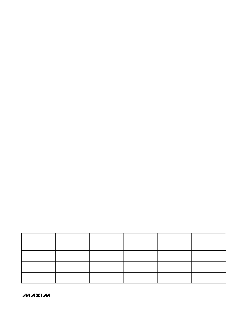
Table 4 shows how the choice of reference-buffer com-
pensation and power-down mode affects both power-up
delay and maximum sample rate. In external compensa-
tion mode, power-up time is 20ms with a 4.7μF compen-
sation capacitor when the capacitor is initially fully
discharged. From fast power-down, start-up time can be
eliminated by using low-leakage capacitors that do not
discharge more than 1/2LSB while shut down. In power-
down, leakage currents at VREF cause droop on the ref-
erence bypass capacitor. Figures 11a and 11b show
the various power-down sequences in both external and
internal clock modes.
Software Power-Down
Software power-down is activated using bits PD1 and PD0
of the control byte. As shown in Table 5, PD1 and PD0
also specify the clock mode. When software shutdown is
asserted, the ADC operates in the last specified clock
mode until the conversion is complete. Then the ADC
powers down into a low quiescent-current state. In internal
clock mode, the interface remains active and conversion
results may be clocked out after the MAX1246/MAX1247
enter a software power-down.
The first logical 1 on DIN is interpreted as a start bit
and powers up the MAX1246/MAX1247. Following
the start bit, the data input word or control byte also
REFERENCE
BUFFER
REFERENCE-
BUFFER
COMPENSATION
MODE
Internal
Internal
External
External
VREF
CAPACITOR
(μF)
POWER-DOWN
MODE
POWER-UP
DELAY
(μs)
MAXIMUM
SAMPLING RATE
(ksps)
Enabled
Enabled
Enabled
Enabled
Disabled
Disabled
Fast
Full
Fast
Full
Fast
Full
5
26
26
133
133
133
133
300
4.7
4.7
See Figure 13c
See Figure 13c
2
2
Table 4. Typical Power-Up Delay Times
相关PDF资料 |
PDF描述 |
|---|---|
| MAX1247BCEE | +2.7V, Low-Power, 4-Channel, Serial 12-Bit ADCs in QSOP-16 |
| MAX1247BEEE | +2.7V, Low-Power, 4-Channel, Serial 12-Bit ADCs in QSOP-16 |
| MAX1246BEEE | +2.7V, Low-Power, 4-Channel, Serial 12-Bit ADCs in QSOP-16 |
| MAX1253AEUE | Stand-Alone, 10-Channel, 12-Bit System Monitors with Internal Temperature Sensor and VDD Monitor |
| MAX1253 | Stand-Alone. 10-Channel. 12-Bit System Monitors with Internal Temperature Sensor and VDD Monitor |
相关代理商/技术参数 |
参数描述 |
|---|---|
| MAX1246ACEE+ | 功能描述:模数转换器 - ADC 12-Bit 4Ch 133ksps 3.6V Precision ADC RoHS:否 制造商:Texas Instruments 通道数量:2 结构:Sigma-Delta 转换速率:125 SPs to 8 KSPs 分辨率:24 bit 输入类型:Differential 信噪比:107 dB 接口类型:SPI 工作电源电压:1.7 V to 3.6 V, 2.7 V to 5.25 V 最大工作温度:+ 85 C 安装风格:SMD/SMT 封装 / 箱体:VQFN-32 |
| MAX1246ACEE+T | 功能描述:模数转换器 - ADC 12-Bit 4Ch 133ksps 3.6V Precision ADC RoHS:否 制造商:Texas Instruments 通道数量:2 结构:Sigma-Delta 转换速率:125 SPs to 8 KSPs 分辨率:24 bit 输入类型:Differential 信噪比:107 dB 接口类型:SPI 工作电源电压:1.7 V to 3.6 V, 2.7 V to 5.25 V 最大工作温度:+ 85 C 安装风格:SMD/SMT 封装 / 箱体:VQFN-32 |
| MAX1246ACEE-T | 功能描述:模数转换器 - ADC RoHS:否 制造商:Texas Instruments 通道数量:2 结构:Sigma-Delta 转换速率:125 SPs to 8 KSPs 分辨率:24 bit 输入类型:Differential 信噪比:107 dB 接口类型:SPI 工作电源电压:1.7 V to 3.6 V, 2.7 V to 5.25 V 最大工作温度:+ 85 C 安装风格:SMD/SMT 封装 / 箱体:VQFN-32 |
| MAX1246ACPE | 功能描述:模数转换器 - ADC RoHS:否 制造商:Texas Instruments 通道数量:2 结构:Sigma-Delta 转换速率:125 SPs to 8 KSPs 分辨率:24 bit 输入类型:Differential 信噪比:107 dB 接口类型:SPI 工作电源电压:1.7 V to 3.6 V, 2.7 V to 5.25 V 最大工作温度:+ 85 C 安装风格:SMD/SMT 封装 / 箱体:VQFN-32 |
| MAX1246ACPE+ | 功能描述:模数转换器 - ADC 12-Bit 4Ch 133ksps 3.6V Precision ADC RoHS:否 制造商:Texas Instruments 通道数量:2 结构:Sigma-Delta 转换速率:125 SPs to 8 KSPs 分辨率:24 bit 输入类型:Differential 信噪比:107 dB 接口类型:SPI 工作电源电压:1.7 V to 3.6 V, 2.7 V to 5.25 V 最大工作温度:+ 85 C 安装风格:SMD/SMT 封装 / 箱体:VQFN-32 |
发布紧急采购,3分钟左右您将得到回复。