- 您现在的位置:买卖IC网 > PDF目录17011 > MAX1246EVKIT (Maxim Integrated Products)EVALUATION KIT FOR MAX1246 PDF资料下载
参数资料
| 型号: | MAX1246EVKIT |
| 厂商: | Maxim Integrated Products |
| 文件页数: | 4/25页 |
| 文件大小: | 0K |
| 描述: | EVALUATION KIT FOR MAX1246 |
| 产品培训模块: | Lead (SnPb) Finish for COTS Obsolescence Mitigation Program |
| 标准包装: | 1 |
| ADC 的数量: | 1 |
| 位数: | 12 |
| 采样率(每秒): | 133k |
| 数据接口: | 串行 |
| 输入范围: | ±VREF/2 |
| 在以下条件下的电源(标准): | 3.6mW @ 133kSPS |
| 工作温度: | 0°C ~ 70°C |
| 已用 IC / 零件: | MAX1246 |
| 已供物品: | 板,CD |

MAX1246/MAX1247
+2.7V, Low-Power, 4-Channel,
Serial 12-Bit ADCs in QSOP-16
12
______________________________________________________________________________________
Circuit, the simplest software interface requires only
three 8-bit transfers to perform a conversion (one 8-bit
transfer to configure the ADC, and two more 8-bit trans-
fers to clock out the 12-bit conversion result). See Figure
19 for MAX1246/MAX1247 QSPI connections.
Simple Software Interface
Make sure the CPU’s serial interface runs in master
mode so the CPU generates the serial clock. Choose a
clock frequency from 100kHz to 2MHz.
1) Set up the control byte for external clock mode and
call it TB1. TB1 should be of the format: 1XXXXX11
binary, where the Xs denote the particular channel
and conversion mode selected.
2) Use a general-purpose I/O line on the CPU to pull
CS low.
3) Transmit TB1 and, simultaneously, receive a byte
and call it RB1. Ignore RB1.
4) Transmit a byte of all zeros ($00 hex) and, simulta-
neously, receive byte RB2.
5) Transmit a byte of all zeros ($00 hex) and, simulta-
neously, receive byte RB3.
6) Pull CS high.
Figure 5 shows the timing for this sequence. Bytes RB2
and RB3 contain the result of the conversion, padded
with one leading zero and three trailing zeros. The total
conversion time is a function of the serial-clock fre-
quency and the amount of idle time between 8-bit
transfers. To avoid excessive T/H droop, make sure the
total conversion time does not exceed 120s.
Digital Output
In unipolar input mode, the output is straight binary
(Figure 16). For bipolar inputs, the output is two’s com-
plement (Figure 17). Data is clocked out at the falling
edge of SCLK in MSB-first format.
Clock Modes
The MAX1246/MAX1247 may use either an external
serial clock or the internal clock to perform the succes-
sive-approximation conversion. In both clock modes,
the external clock shifts data in and out of the
MAX1246/MAX1247. The T/H acquires the input signal
as the last three bits of the control byte are clocked into
DIN. Bits PD1 and PD0 of the control byte program the
clock mode. Figures 6–9 show the timing characteristics
common to both modes.
External Clock
In external clock mode, the external clock not only shifts
data in and out, but it also drives the analog-to-digital
conversion steps. SSTRB pulses high for one clock
period after the last bit of the control byte. Succes-
sive-approximation bit decisions are made and appear
at DOUT on each of the next 12 SCLK falling edges
(Figure 5). SSTRB and DOUT go into a high-impedance
state when CS goes high; after the next CS falling edge,
SSTRB outputs a logic low. Figure 7 shows the SSTRB
timing in external clock mode.
The conversion must complete in some minimum time,
or droop on the sample-and-hold capacitors may
degrade conversion results. Use internal clock mode if
the serial clock frequency is less than 100kHz, or if
serial clock interruptions could cause the conversion
interval to exceed 120s.
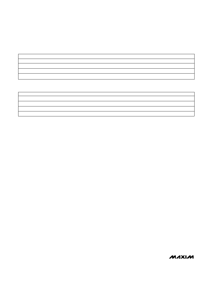
SEL2
SEL1
SEL0
CH0
CH1
CH2
CH3
COM
00
1
+
–
10
1
+
–
01
0
+
–
11
0
+
–
Table 2. Channel Selection in Single-Ended Mode (SGL/D
DIIF
F = 1)
SEL2
SEL1
SEL0
CH0
CH1
CH2
CH3
00
1
+
–
01
0
+
–
10
1
–
+
11
0
–
+
Table 3. Channel Selection in Differential Mode (SGL/D
DIIF
F = 0)
相关PDF资料 |
PDF描述 |
|---|---|
| GBM25DTBS | CONN EDGECARD 50POS R/A .156 SLD |
| PCM16YC0 | PROCESSOR MODULE FOR PIC16C433 |
| PCM16YB0 | PROCESSOR MODULE FOR PIC16C432 |
| MAX1202EVKIT | EVALUATION KIT FOR MAX1202 |
| GBM18DTAT | CONN EDGECARD 36POS R/A .156 SLD |
相关代理商/技术参数 |
参数描述 |
|---|---|
| MAX1246EVL11-QSOP | 功能描述:数据转换 IC 开发工具 MAX1246 Eval Kit RoHS:否 制造商:Texas Instruments 产品:Demonstration Kits 类型:ADC 工具用于评估:ADS130E08 接口类型:SPI 工作电源电压:- 6 V to + 6 V |
| MAX1247ACEE | 功能描述:模数转换器 - ADC Integrated Circuits (ICs) RoHS:否 制造商:Texas Instruments 通道数量:2 结构:Sigma-Delta 转换速率:125 SPs to 8 KSPs 分辨率:24 bit 输入类型:Differential 信噪比:107 dB 接口类型:SPI 工作电源电压:1.7 V to 3.6 V, 2.7 V to 5.25 V 最大工作温度:+ 85 C 安装风格:SMD/SMT 封装 / 箱体:VQFN-32 |
| MAX1247ACEE+ | 功能描述:模数转换器 - ADC 12-Bit 4Ch 133ksps 5.25V Precision ADC RoHS:否 制造商:Texas Instruments 通道数量:2 结构:Sigma-Delta 转换速率:125 SPs to 8 KSPs 分辨率:24 bit 输入类型:Differential 信噪比:107 dB 接口类型:SPI 工作电源电压:1.7 V to 3.6 V, 2.7 V to 5.25 V 最大工作温度:+ 85 C 安装风格:SMD/SMT 封装 / 箱体:VQFN-32 |
| MAX1247ACEE+T | 功能描述:模数转换器 - ADC 12-Bit 4Ch 133ksps 5.25V Precision ADC RoHS:否 制造商:Texas Instruments 通道数量:2 结构:Sigma-Delta 转换速率:125 SPs to 8 KSPs 分辨率:24 bit 输入类型:Differential 信噪比:107 dB 接口类型:SPI 工作电源电压:1.7 V to 3.6 V, 2.7 V to 5.25 V 最大工作温度:+ 85 C 安装风格:SMD/SMT 封装 / 箱体:VQFN-32 |
| MAX1247ACEE-T | 功能描述:模数转换器 - ADC RoHS:否 制造商:Texas Instruments 通道数量:2 结构:Sigma-Delta 转换速率:125 SPs to 8 KSPs 分辨率:24 bit 输入类型:Differential 信噪比:107 dB 接口类型:SPI 工作电源电压:1.7 V to 3.6 V, 2.7 V to 5.25 V 最大工作温度:+ 85 C 安装风格:SMD/SMT 封装 / 箱体:VQFN-32 |
发布紧急采购,3分钟左右您将得到回复。