- 您现在的位置:买卖IC网 > PDF目录383316 > MAX1247BMJE (MAXIM INTEGRATED PRODUCTS INC) +2.7V, Low-Power, 4-Channel, Serial 12-Bit ADCs in QSOP-16 PDF资料下载
参数资料
| 型号: | MAX1247BMJE |
| 厂商: | MAXIM INTEGRATED PRODUCTS INC |
| 元件分类: | ADC |
| 英文描述: | +2.7V, Low-Power, 4-Channel, Serial 12-Bit ADCs in QSOP-16 |
| 中文描述: | 4-CH 12-BIT SUCCESSIVE APPROXIMATION ADC, SERIAL ACCESS, CDIP16 |
| 封装: | CERDIP-16 |
| 文件页数: | 20/24页 |
| 文件大小: | 223K |
| 代理商: | MAX1247BMJE |
M
+2.7V, Low-Power, 4-Channel,
S erial 12-Bit ADCs in QS OP-16
20
______________________________________________________________________________________
T MS 320LC3x Interfac e
Figure 20 shows an application circuit to interface the
MAX1246/MAX1247 to the TMS320 in external clock
mode. The timing diagram for this interface circuit is
shown in Figure 21.
Use the following steps to initiate a conversion in the
MAX1246/MAX1247 and to read the results:
1)
The TMS320 should be configured with CLKX
(transmit clock) as an active-high output clock and
CLKR (TMS320 receive clock) as an active-high
input clock. CLKX and CLKR on the TMS320 are
tied together with the MAX1246/MAX1247’s SCLK
input.
2)
The MAX1246/MAX1247’s
CS
pin is driven low by
the TMS320’s XF_ I/O port to enable data to be
clocked into the MAX1246/MAX1247’s DIN.
3)
An 8-bit word (1XXXXX11) should be written to the
MAX1246/MAX1247 to initiate a conversion and
place the device into external clock mode. Refer to
Table 1 to select the proper XXXXX bit values for
your specific application.
4)
The MAX1246/MAX1247’s SSTRB output is moni-
tored via the TMS320’s FSR input. A falling edge on
the SSTRB output indicates that the conversion is in
progress and data is ready to be received from the
MAX1246/MAX1247.
The TMS320 reads in one data bit on each of the
next 16 rising edges of SCLK. These data bits rep-
resent the 12-bit conversion result followed by four
trailing bits, which should be ignored.
Pull
CS
high to disable the MAX1246/MAX1247 until
the next conversion is initiated.
5)
6)
011
. . .
111
011
. . .
110
000
. . .
010
000
. . .
001
000
. . .
000
111
. . .
111
111
. . .
110
111
. . .
101
100
. . .
001
100
. . .
000
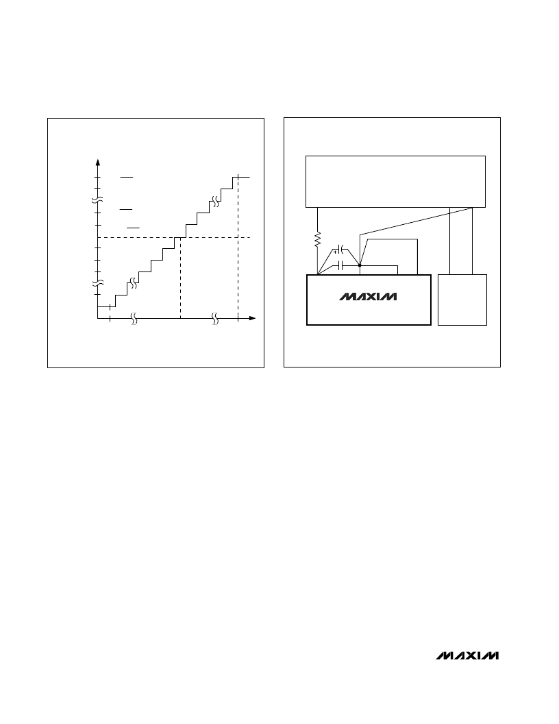
- FS
COM*
INPUT VOLTAGE (LSB)
OUTPUT CODE
ZS = COM
+FS - 1LSB
*COM VREF / 2
+ COM
FS
= V2
-FS =
+ COM
-VREF
2
1LSB = 4096
Figure 17. Bipolar Transfer Function, Full Scale (FS) =
VREF / 2 + COM, Zero Scale (ZS) = COM
+3V
+3V
GND
SUPPLIES
DGND
+3V
DGND
COM
AGND
V
DD
DIGITAL
CIRCUITRY
MAX1246
MAX1247
R* = 10
*OPTIONAL
Figure 18. Power-Supply Grounding Connection
相关PDF资料 |
PDF描述 |
|---|---|
| MAX1246 | +2.7V, Low-Power, 4-Channel, Serial 12-Bit ADCs in QSOP-16 |
| MAX1246ACEE | +2.7V, Low-Power, 4-Channel, Serial 12-Bit ADCs in QSOP-16 |
| MAX1247BCEE | +2.7V, Low-Power, 4-Channel, Serial 12-Bit ADCs in QSOP-16 |
| MAX1247BEEE | +2.7V, Low-Power, 4-Channel, Serial 12-Bit ADCs in QSOP-16 |
| MAX1246BEEE | +2.7V, Low-Power, 4-Channel, Serial 12-Bit ADCs in QSOP-16 |
相关代理商/技术参数 |
参数描述 |
|---|---|
| MAX1247CCEE | 制造商:Rochester Electronics LLC 功能描述: 制造商:Maxim Integrated Products 功能描述: |
| MAX1247CCPE | 制造商:Rochester Electronics LLC 功能描述: 制造商:Maxim Integrated Products 功能描述: |
| MAX1247CEEE | 制造商:Rochester Electronics LLC 功能描述: 制造商:Maxim Integrated Products 功能描述: |
| MAX1247EVKIT | 功能描述:数据转换 IC 开发工具 MAX1247 Eval Kit RoHS:否 制造商:Texas Instruments 产品:Demonstration Kits 类型:ADC 工具用于评估:ADS130E08 接口类型:SPI 工作电源电压:- 6 V to + 6 V |
| MAX1247EVL11-QSOP | 功能描述:数据转换 IC 开发工具 MAX1247L11-QSOP Eval Kit RoHS:否 制造商:Texas Instruments 产品:Demonstration Kits 类型:ADC 工具用于评估:ADS130E08 接口类型:SPI 工作电源电压:- 6 V to + 6 V |
发布紧急采购,3分钟左右您将得到回复。