- 您现在的位置:买卖IC网 > PDF目录2008 > MAX1249AEPE+ (Maxim Integrated Products)IC ADC 10BIT SERIAL 16-DIP PDF资料下载
参数资料
| 型号: | MAX1249AEPE+ |
| 厂商: | Maxim Integrated Products |
| 文件页数: | 13/24页 |
| 文件大小: | 0K |
| 描述: | IC ADC 10BIT SERIAL 16-DIP |
| 产品培训模块: | Lead (SnPb) Finish for COTS Obsolescence Mitigation Program |
| 标准包装: | 25 |
| 位数: | 10 |
| 采样率(每秒): | 133k |
| 数据接口: | MICROWIRE?,QSPI?,串行,SPI? |
| 转换器数目: | 1 |
| 功率耗散(最大): | 842mW |
| 电压电源: | 单电源 |
| 工作温度: | -40°C ~ 85°C |
| 安装类型: | 通孔 |
| 封装/外壳: | 16-DIP(0.300",7.62mm) |
| 供应商设备封装: | 16-PDIP |
| 包装: | 管件 |
| 输入数目和类型: | 4 个单端,单极;4 个单端,双极;2 个差分,单极;2 个差分,双极 |
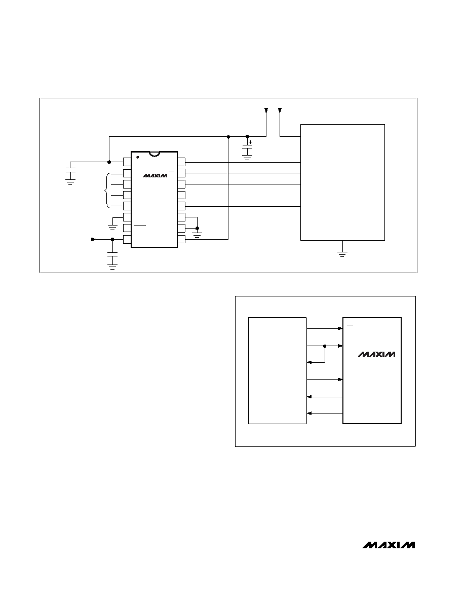
MAX1248/MAX1249
TMS320LC3x Interface
Figure 20 shows an application circuit to interface the
MAX1248/MAX1249 to the TMS320 in external clock
mode. The timing diagram for this interface circuit is
shown in Figure 21.
Use the following steps to initiate a conversion in the
MAX1248/MAX1249 and to read the results:
1) The TMS320 should be configured with CLKX
(transmit clock) as an active-high output clock and
CLKR (TMS320 receive clock) as an active-high
input clock. CLKX and CLKR on the TMS320 are
tied together with the MAX1248/MAX1249’s SCLK
input.
2) The MAX1248/MAX1249’s CS pin is driven low by
the TMS320’s XF_ I/O port, to enable data to be
clocked into the MAX1248/MAX1249’s DIN.
3) An 8-bit word (1XXXXX11) should be written to the
MAX1248/MAX1249 to initiate a conversion and
place the device into external clock mode. Refer to
Table 1 to select the proper XXXXX bit values for
your specific application.
4) The MAX1248/MAX1249’s SSTRB output is moni-
tored via the TMS320’s FSR input. A falling edge on
the SSTRB output indicates that the conversion is in
progress and data is ready to be received from the
MAX1248/MAX1249.
5) The TMS320 reads in one data bit on each of the
next 16 rising edges of SCLK. These data bits rep-
resent the 10 + 2-bit conversion result followed by
four trailing bits, which should be ignored.
6) Pull CS high to disable the MAX1248/MAX1249 until
the next conversion is initiated.
+2.7V to +5.25V, Low-Power, 4-Channel,
Serial 10-Bit ADCs in QSOP-16
20
______________________________________________________________________________________
16
15
14
13
12
11
10
9
1
2
3
4
5
6
7
8
MAX1248
MAX1249
MC683XX
SCK
PCS0
MOSI
MISO
CLOCK CONNECTIONS NOT SHOWN
1
F
0.1
F
0.1
F
(GND)
ANALOG
INPUTS
+3V
VDD
CH0
CH1
CH2
CH3
COM
SHDN
VREF
SCLK
CS
DIN
SSTRB
DOUT
DGND
AGND
REFADJ
+2.5V
XF
CLKX
CLKR
DX
DR
FSR
CS
SCLK
DIN
DOUT
SSTRB
TMS320LC3x
MAX1249
Figure 20. MAX1248/MAX1249-to-TMS320 Serial Interface
Figure 19. MAX1248/MAX1249 QSPI Connections External Reference
相关PDF资料 |
PDF描述 |
|---|---|
| MAX1279AETC+ | IC ADC 12BIT 1.5MSPS 12-TQFN |
| MAX1285BESA+T | IC ADC 12BIT 300KSPS 8-SOIC |
| MAX1302BEUG+ | IC ADC 16BIT SRL 115KSPS 24TSSOP |
| MAX1303BEUP+ | IC ADC 16BIT MULT RANGE 20TSSOP |
| MAX1308ECM+T | IC ADC 12BIT 8CH 4MSPS 48LQFP |
相关代理商/技术参数 |
参数描述 |
|---|---|
| MAX1249AEPE+ | 功能描述:模数转换器 - ADC 10-Bit 4Ch 133ksps 5.25V Precision ADC RoHS:否 制造商:Texas Instruments 通道数量:2 结构:Sigma-Delta 转换速率:125 SPs to 8 KSPs 分辨率:24 bit 输入类型:Differential 信噪比:107 dB 接口类型:SPI 工作电源电压:1.7 V to 3.6 V, 2.7 V to 5.25 V 最大工作温度:+ 85 C 安装风格:SMD/SMT 封装 / 箱体:VQFN-32 |
| MAX1249AMJE | 功能描述:模数转换器 - ADC RoHS:否 制造商:Texas Instruments 通道数量:2 结构:Sigma-Delta 转换速率:125 SPs to 8 KSPs 分辨率:24 bit 输入类型:Differential 信噪比:107 dB 接口类型:SPI 工作电源电压:1.7 V to 3.6 V, 2.7 V to 5.25 V 最大工作温度:+ 85 C 安装风格:SMD/SMT 封装 / 箱体:VQFN-32 |
| MAX1249BCEE | 功能描述:模数转换器 - ADC RoHS:否 制造商:Texas Instruments 通道数量:2 结构:Sigma-Delta 转换速率:125 SPs to 8 KSPs 分辨率:24 bit 输入类型:Differential 信噪比:107 dB 接口类型:SPI 工作电源电压:1.7 V to 3.6 V, 2.7 V to 5.25 V 最大工作温度:+ 85 C 安装风格:SMD/SMT 封装 / 箱体:VQFN-32 |
| MAX1249BCEE+ | 功能描述:模数转换器 - ADC 10-Bit 4Ch 133ksps 5.25V Precision ADC RoHS:否 制造商:Texas Instruments 通道数量:2 结构:Sigma-Delta 转换速率:125 SPs to 8 KSPs 分辨率:24 bit 输入类型:Differential 信噪比:107 dB 接口类型:SPI 工作电源电压:1.7 V to 3.6 V, 2.7 V to 5.25 V 最大工作温度:+ 85 C 安装风格:SMD/SMT 封装 / 箱体:VQFN-32 |
| MAX1249BCEE+T | 功能描述:模数转换器 - ADC 10-Bit 4Ch 133ksps 5.25V Precision ADC RoHS:否 制造商:Texas Instruments 通道数量:2 结构:Sigma-Delta 转换速率:125 SPs to 8 KSPs 分辨率:24 bit 输入类型:Differential 信噪比:107 dB 接口类型:SPI 工作电源电压:1.7 V to 3.6 V, 2.7 V to 5.25 V 最大工作温度:+ 85 C 安装风格:SMD/SMT 封装 / 箱体:VQFN-32 |
发布紧急采购,3分钟左右您将得到回复。