- 您现在的位置:买卖IC网 > PDF目录2008 > MAX1249AEPE+ (Maxim Integrated Products)IC ADC 10BIT SERIAL 16-DIP PDF资料下载
参数资料
| 型号: | MAX1249AEPE+ |
| 厂商: | Maxim Integrated Products |
| 文件页数: | 4/24页 |
| 文件大小: | 0K |
| 描述: | IC ADC 10BIT SERIAL 16-DIP |
| 产品培训模块: | Lead (SnPb) Finish for COTS Obsolescence Mitigation Program |
| 标准包装: | 25 |
| 位数: | 10 |
| 采样率(每秒): | 133k |
| 数据接口: | MICROWIRE?,QSPI?,串行,SPI? |
| 转换器数目: | 1 |
| 功率耗散(最大): | 842mW |
| 电压电源: | 单电源 |
| 工作温度: | -40°C ~ 85°C |
| 安装类型: | 通孔 |
| 封装/外壳: | 16-DIP(0.300",7.62mm) |
| 供应商设备封装: | 16-PDIP |
| 包装: | 管件 |
| 输入数目和类型: | 4 个单端,单极;4 个单端,双极;2 个差分,单极;2 个差分,双极 |
MAX1248/MAX1249
+2.7V to +5.25V, Low-Power, 4-Channel,
Serial 10-Bit ADCs in QSOP-16
12
______________________________________________________________________________________
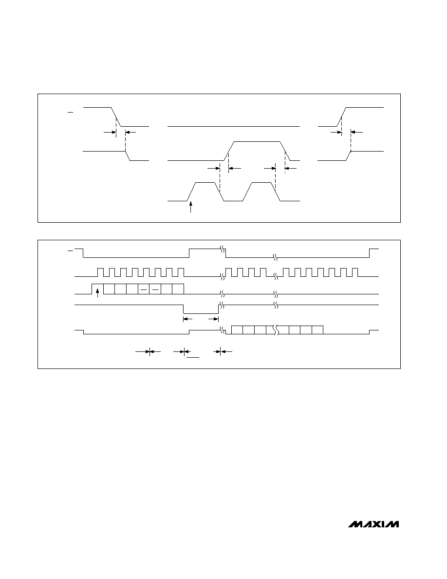
Internal Clock
In internal clock mode, the MAX1248/MAX1249 gener-
ate their own conversion clocks internally. This frees the
P from the burden of running the SAR conversion clock
and allows the conversion results to be read back at the
processor’s convenience, at any clock rate from 0MHz
to 2MHz. SSTRB goes low at the start of the conversion
and then goes high when the conversion is complete.
SSTRB is low for a maximum of 7.5s (SHDN = FLOAT),
during which time SCLK should remain low for best
noise performance.
An internal register stores data when the conversion is
in progress. SCLK clocks the data out of this register at
any time after the conversion is complete. After SSTRB
goes high, the next falling clock edge produces the
MSB of the conversion at DOUT, followed by the
remaining bits in MSB-first format (Figure 8). CS does
not need to be held low once a conversion is started.
Pulling CS high prevents data from being clocked into
the MAX1248/MAX1249 and three-states DOUT, but it
does not adversely affect an internal clock mode con-
version already in progress. When internal clock mode
is selected, SSTRB does not go into a high-impedance
state when CS goes high.
Figure 9 shows the SSTRB timing in internal clock
mode. In this mode, data can be shifted in and out of
the MAX1248/MAX1249 at clock rates exceeding
2.0MHz if the minimum acquisition time, tACQ, is kept
above 1.5s.
SSTRB
CS
SCLK
DIN
DOUT
1
4
8
12
18
20
24
START
SEL2 SEL1 SEL0
UNI/
BIP
SGL/
DIF
PD1 PD0
B9
MSB
B8
B7
B0
LSB
S1
S0
FILLED WITH
ZEROS
IDLE
CONVERSION
7.5s MAX
(SHDN = FLOAT)
2
3
5
6
7
9
10
11
19
21
22
23
tCONV
ACQUISITION
(fSCLK = 2MHz)
IDLE
A/D STATE
1.5s
Figure 8. Internal Clock Mode Timing
tSDV
tSSTRB
PD0 CLOCKED IN
tSTR
SSTRB
SCLK
CS
tSSTRB
Figure 7. External Clock Mode SSTRB Detailed Timing
相关PDF资料 |
PDF描述 |
|---|---|
| MAX1279AETC+ | IC ADC 12BIT 1.5MSPS 12-TQFN |
| MAX1285BESA+T | IC ADC 12BIT 300KSPS 8-SOIC |
| MAX1302BEUG+ | IC ADC 16BIT SRL 115KSPS 24TSSOP |
| MAX1303BEUP+ | IC ADC 16BIT MULT RANGE 20TSSOP |
| MAX1308ECM+T | IC ADC 12BIT 8CH 4MSPS 48LQFP |
相关代理商/技术参数 |
参数描述 |
|---|---|
| MAX1249AEPE+ | 功能描述:模数转换器 - ADC 10-Bit 4Ch 133ksps 5.25V Precision ADC RoHS:否 制造商:Texas Instruments 通道数量:2 结构:Sigma-Delta 转换速率:125 SPs to 8 KSPs 分辨率:24 bit 输入类型:Differential 信噪比:107 dB 接口类型:SPI 工作电源电压:1.7 V to 3.6 V, 2.7 V to 5.25 V 最大工作温度:+ 85 C 安装风格:SMD/SMT 封装 / 箱体:VQFN-32 |
| MAX1249AMJE | 功能描述:模数转换器 - ADC RoHS:否 制造商:Texas Instruments 通道数量:2 结构:Sigma-Delta 转换速率:125 SPs to 8 KSPs 分辨率:24 bit 输入类型:Differential 信噪比:107 dB 接口类型:SPI 工作电源电压:1.7 V to 3.6 V, 2.7 V to 5.25 V 最大工作温度:+ 85 C 安装风格:SMD/SMT 封装 / 箱体:VQFN-32 |
| MAX1249BCEE | 功能描述:模数转换器 - ADC RoHS:否 制造商:Texas Instruments 通道数量:2 结构:Sigma-Delta 转换速率:125 SPs to 8 KSPs 分辨率:24 bit 输入类型:Differential 信噪比:107 dB 接口类型:SPI 工作电源电压:1.7 V to 3.6 V, 2.7 V to 5.25 V 最大工作温度:+ 85 C 安装风格:SMD/SMT 封装 / 箱体:VQFN-32 |
| MAX1249BCEE+ | 功能描述:模数转换器 - ADC 10-Bit 4Ch 133ksps 5.25V Precision ADC RoHS:否 制造商:Texas Instruments 通道数量:2 结构:Sigma-Delta 转换速率:125 SPs to 8 KSPs 分辨率:24 bit 输入类型:Differential 信噪比:107 dB 接口类型:SPI 工作电源电压:1.7 V to 3.6 V, 2.7 V to 5.25 V 最大工作温度:+ 85 C 安装风格:SMD/SMT 封装 / 箱体:VQFN-32 |
| MAX1249BCEE+T | 功能描述:模数转换器 - ADC 10-Bit 4Ch 133ksps 5.25V Precision ADC RoHS:否 制造商:Texas Instruments 通道数量:2 结构:Sigma-Delta 转换速率:125 SPs to 8 KSPs 分辨率:24 bit 输入类型:Differential 信噪比:107 dB 接口类型:SPI 工作电源电压:1.7 V to 3.6 V, 2.7 V to 5.25 V 最大工作温度:+ 85 C 安装风格:SMD/SMT 封装 / 箱体:VQFN-32 |
发布紧急采购,3分钟左右您将得到回复。