参数资料
| 型号: | MAX1271BEAI+ |
| 厂商: | Maxim Integrated Products |
| 文件页数: | 4/20页 |
| 文件大小: | 0K |
| 描述: | IC ADC 12BIT 8CH 28-SSOP |
| 产品培训模块: | Lead (SnPb) Finish for COTS Obsolescence Mitigation Program |
| 标准包装: | 46 |
| 类型: | 数据采集系统(DAS),ADC |
| 分辨率(位): | 12 b |
| 采样率(每秒): | 110k |
| 数据接口: | 串行 |
| 电压电源: | 单电源 |
| 电源电压: | 4.75 V ~ 5.25 V |
| 工作温度: | -40°C ~ 85°C |
| 安装类型: | 表面贴装 |
| 封装/外壳: | 28-SSOP(0.209",5.30mm 宽) |
| 供应商设备封装: | 28-SSOP |
| 包装: | 管件 |
| 产品目录页面: | 1396 (CN2011-ZH PDF) |
MAX1270/MAX1271
Multirange, +5V, 8-Channel,
Serial 12-Bit ADCs
12
______________________________________________________________________________________
Input Data Format
Input data (control byte) is clocked in at DIN at the ris-
ing edge of SCLK. CS enables communication with the
MAX1270/MAX1271. After CS falls, the first arriving
logic 1 bit represents the start bit (MSB) of the input
control byte. The start bit is defined as:
The first high bit clocked into DIN with CS low
anytime the converter is idle; e.g., after VDD is
applied.
OR
The first high bit clocked into DIN after bit 6
(D6) of a conversion in progress is clocked
onto DOUT.
Output Data Format
Output data is clocked out on the falling edge of SCLK
at DOUT, MSB first (D11). In unipolar mode, the output
is straight binary. For bipolar mode, the output is two’s
complement binary. For output binary codes, refer to
the Transfer Function section.
How to Start a Conversion
The MAX1270/MAX1271 use either an external serial
clock or the internal clock to complete an acquisition
and perform a conversion. In both clock modes, the
external clock shifts data in and out. See Table 4 for
details on programming clock modes.
The falling edge of CS does not start a conversion on
the MAX1270/MAX1271; a control byte is required for
each conversion. Acquisition starts after the sixth bit is
programmed in the input control byte. Conversion
starts when the acquisition time, six clock cycles,
expires.
Keep CS low during successive conversions. If a start-
bit is received after CS transitions from high to low, but
before the output bit 6 (D6) becomes available, the cur-
rent conversion will terminate and a new conversion will
begin.
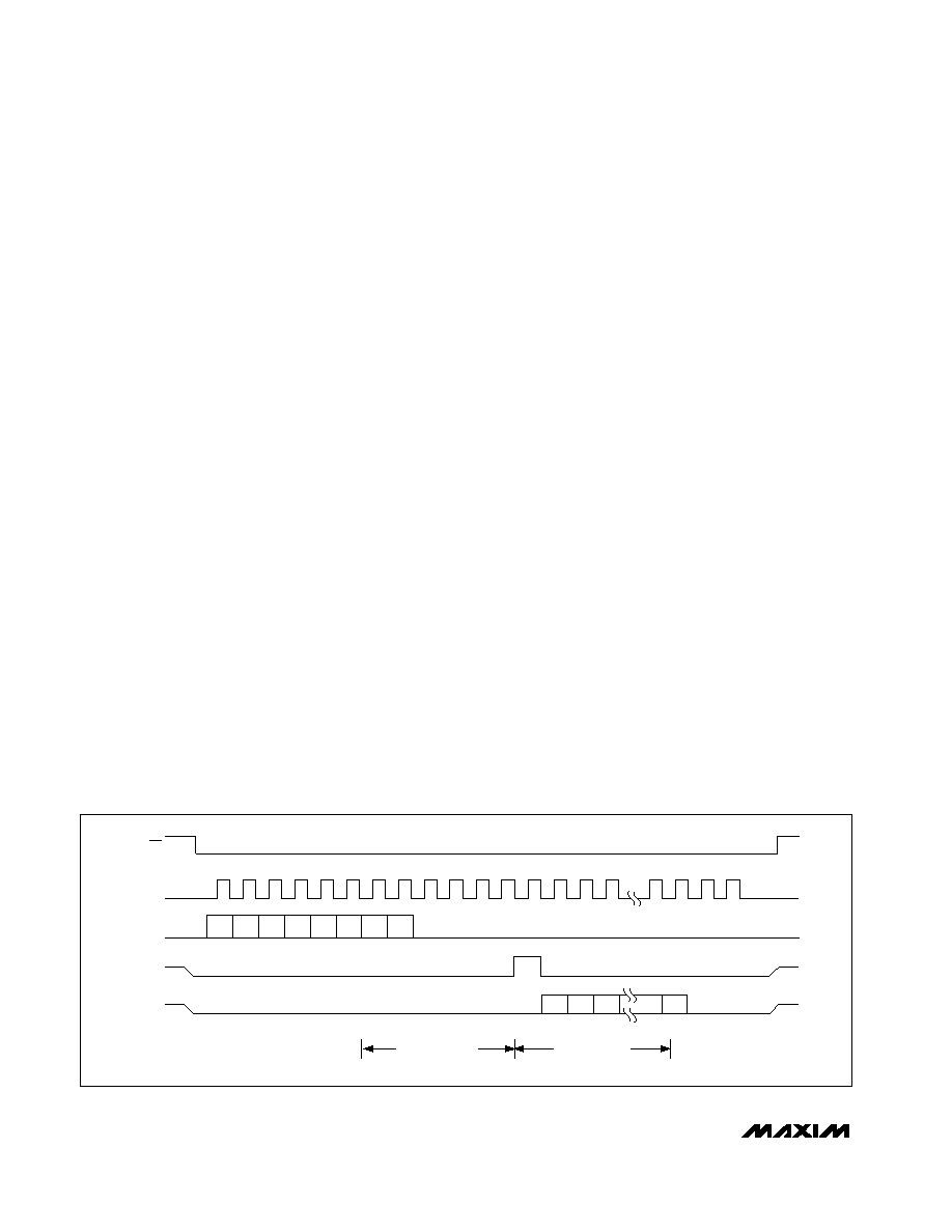
External Clock Mode (PD1 = 0, PD0 = 1)
In external clock mode, the clock shifts data in and out
of the MAX1270/MAX1271 and controls the acquisition
and conversion timings. When acquisition is done,
SSTRB pulses high for one clock cycle and conversion
begins. Successive-approximation bit decisions appear
at DOUT on each of the next 12 SCLK falling edges
(Figure 6). Additional SCLK falling edges will result in
zeros appearing at DOUT. Figure 7 shows the SSTRB
timing in external clock mode.
SSTRB and DOUT go into a high-impedance state
when CS goes high; after the next CS falling edge,
SSTRB and DOUT will output a logic low.
The conversion must be completed in some minimum
time, or droop on the sample-and-hold capacitors may
degrade conversion results. Use internal clock mode if
the clock period exceeds 10s, or if serial-clock inter-
ruptions could cause the conversion interval to exceed
120s. The fastest the MAX1270/MAX1271 can run is
18 clocks per conversion in external clock mode, and
with a clock rate of 2MHz, the maximum sampling rate
is 111 ksps (Figure 8). In order to achieve maximum
throughput, keep CS low, use external clock mode with
a continuous SCLK, and start the following control byte
after bit 6 (D6) of the conversion in progress is clocked
onto DOUT.
If CS is low and SCLK is continuous, guarantee a start
bit by first clocking in 18 zeros.
SSTRB
CS
SCLK
DIN
DOUT
18
12
13
14
24
25
START SEL2 SEL1 SEL0
BIP
RNG
PD1
PD0
LSB
D11
MSB
D10
D9
D1
D0
LSB
ACQUISITION
6 SCLK
FILLED WITH
ZEROS
CONVERSION
12 SCLK
A/D STATE
HIGH-Z
Figure 6. External Clock Mode—25 Clocks/Conversion Timing
相关PDF资料 |
PDF描述 |
|---|---|
| MAX1270BEAI+ | IC ADC 12BIT SERIAL 28-SSOP |
| 74VHC139MTCX | DECODER/DEMUX DUAL 2-4 16TSSOP |
| D38999/24FJ7SA | CONN RCPT 99POS JAM NUT W/SCKT |
| VE-BTR-MY-S | CONVERTER MOD DC/DC 7.5V 50W |
| MS27468T25B1SA | CONN RCPT 128POS JAM NUT W/SCKT |
相关代理商/技术参数 |
参数描述 |
|---|---|
| MAX1271BEAI+ | 功能描述:模数转换器 - ADC 12-Bit 8Ch 110ksps 4.18V Precision ADC RoHS:否 制造商:Texas Instruments 通道数量:2 结构:Sigma-Delta 转换速率:125 SPs to 8 KSPs 分辨率:24 bit 输入类型:Differential 信噪比:107 dB 接口类型:SPI 工作电源电压:1.7 V to 3.6 V, 2.7 V to 5.25 V 最大工作温度:+ 85 C 安装风格:SMD/SMT 封装 / 箱体:VQFN-32 |
| MAX1271BEAI+T | 功能描述:模数转换器 - ADC 12-Bit 8Ch 110ksps 4.18V Precision ADC RoHS:否 制造商:Texas Instruments 通道数量:2 结构:Sigma-Delta 转换速率:125 SPs to 8 KSPs 分辨率:24 bit 输入类型:Differential 信噪比:107 dB 接口类型:SPI 工作电源电压:1.7 V to 3.6 V, 2.7 V to 5.25 V 最大工作温度:+ 85 C 安装风格:SMD/SMT 封装 / 箱体:VQFN-32 |
| MAX1271BEAI-T | 功能描述:模数转换器 - ADC RoHS:否 制造商:Texas Instruments 通道数量:2 结构:Sigma-Delta 转换速率:125 SPs to 8 KSPs 分辨率:24 bit 输入类型:Differential 信噪比:107 dB 接口类型:SPI 工作电源电压:1.7 V to 3.6 V, 2.7 V to 5.25 V 最大工作温度:+ 85 C 安装风格:SMD/SMT 封装 / 箱体:VQFN-32 |
| MAX1271BENG | 功能描述:模数转换器 - ADC RoHS:否 制造商:Texas Instruments 通道数量:2 结构:Sigma-Delta 转换速率:125 SPs to 8 KSPs 分辨率:24 bit 输入类型:Differential 信噪比:107 dB 接口类型:SPI 工作电源电压:1.7 V to 3.6 V, 2.7 V to 5.25 V 最大工作温度:+ 85 C 安装风格:SMD/SMT 封装 / 箱体:VQFN-32 |
| MAX1271BENG+ | 功能描述:模数转换器 - ADC 12-Bit 8Ch 110ksps 4.18V Precision ADC RoHS:否 制造商:Texas Instruments 通道数量:2 结构:Sigma-Delta 转换速率:125 SPs to 8 KSPs 分辨率:24 bit 输入类型:Differential 信噪比:107 dB 接口类型:SPI 工作电源电压:1.7 V to 3.6 V, 2.7 V to 5.25 V 最大工作温度:+ 85 C 安装风格:SMD/SMT 封装 / 箱体:VQFN-32 |
发布紧急采购,3分钟左右您将得到回复。