- 您现在的位置:买卖IC网 > PDF目录9902 > MAX1280BEUP+T (Maxim Integrated Products)IC ADC 12BIT 400KSPS 20-TSSOP PDF资料下载
参数资料
| 型号: | MAX1280BEUP+T |
| 厂商: | Maxim Integrated Products |
| 文件页数: | 3/24页 |
| 文件大小: | 0K |
| 描述: | IC ADC 12BIT 400KSPS 20-TSSOP |
| 产品培训模块: | Lead (SnPb) Finish for COTS Obsolescence Mitigation Program |
| 标准包装: | 2,500 |
| 位数: | 12 |
| 采样率(每秒): | 400k |
| 数据接口: | MICROWIRE?,QSPI?,串行,SPI? |
| 转换器数目: | 1 |
| 功率耗散(最大): | 559mW |
| 电压电源: | 单电源 |
| 工作温度: | -40°C ~ 85°C |
| 安装类型: | 表面贴装 |
| 封装/外壳: | 20-TSSOP(0.173",4.40mm 宽) |
| 供应商设备封装: | 20-TSSOP |
| 包装: | 带卷 (TR) |
| 输入数目和类型: | 8 个单端,单极;8 个单端,双极;4 个伪差分,单极;4 个伪差分,双极 |
MAX1280/MAX1281
400ksps/300ksps, Single-Supply, Low-Power, 8-Channel,
Serial 12-Bit ADCs with Internal Reference
______________________________________________________________________________________
11
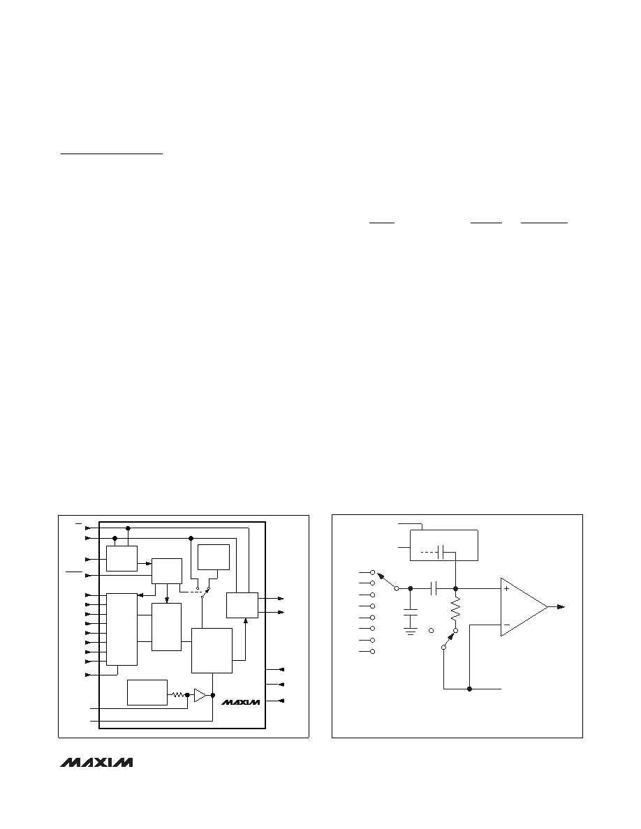
Detailed Description
The MAX1280/MAX1281 analog-to-digital converters
(ADCs) use a successive-approximation conversion tech-
nique and input track/hold (T/H) circuitry to convert an
analog signal to a 12-bit digital output. A flexible serial
interface provides easy interface to microprocessors
(Ps). Figure 3 shows a functional diagram of the
MAX1280/MAX1281.
Pseudo-Differential Input
The equivalent input circuit of Figure 4 shows the
MAX1280/MAX1281’s input architecture, which is com-
posed of a T/H, input multiplexer, input comparator,
switched-capacitor DAC, and reference.
In single-ended mode, the positive input (IN+) is con-
nected to the selected input channel and the negative
input (IN-) is set to COM. In differential mode, IN+ and
IN- are selected from the following pairs: CH0/CH1,
CH2/CH3, CH4/CH5, and CH6/CH7. Configure the
channels according to Tables 2 and 3.
The MAX1280/MAX1281 input configuration is pseudo-
differential in that only the signal at IN+ is sampled. The
return side (IN-) is connected to the sampling capacitor
while converting and must remain stable within ±0.5LSB
(±0.1LSB for best results) with respect to GND during a
conversion.
If a varying signal is applied to the selected IN-, its ampli-
tude and frequency must be limited to maintain accuracy.
The following equations determine the relationship
between the maximum signal amplitude and its frequency
in order to maintain ±0.5LSB accuracy. Assuming a sinu-
soidal signal at IN-, the input voltage is determined by:
The maximum voltage variation is determined by:
A 650mVp-p 60Hz signal at IN- will generate ±0.5LSB
of error when using a +2.5V reference voltage and a
2.5s conversion time (15/fSCLK). When a DC reference
voltage is used at IN-, connect a 0.1F capacitor to
GND to minimize noise at the input.
During the acquisition interval, the channel selected as
the positive input (IN+) charges capacitor CHOLD. The
acquisition interval spans three SCLK cycles and ends
on the falling SCLK edge after the last bit of the input
control word has been entered. At the end of the acqui-
sition interval, the T/H switch opens, retaining charge
on CHOLD as a sample of the signal at IN+. The conver-
sion interval begins with the input multiplexer switching
CHOLD from IN+ to IN-. This unbalances node ZERO at
the comparator’s input. The capacitive DAC adjusts
during the remainder of the conversion cycle to restore
node ZERO to VDD1/2 within the limits of 12-bit
resolution. This action is equivalent to transferring a
12pF x (VIN+ - VIN-) charge from CHOLD to the binary-
weighted capacitive DAC, which in turn forms a digital
representation of the analog input signal.
max
d
-
d
- 2f
1LSB
t
V
2t
IN
t
IN
CONV
REF
12
CONV
ν
π
=
()
≤
=
V
νπ
IN
-- sin(2 ft)
=
()
V
INPUT
SHIFT
REGISTER
CONTROL
LOGIC
INT
CLOCK
OUTPUT
SHIFT
REGISTER
+1.22V
REFERENCE
T/H
ANALOG
INPUT
MUX
12-BIT
SAR
ADC
IN
DOUT
SSTRB
VDD1
VDD2
GND
SCLK
DIN
COM
REFADJ
REF
OUT
REF
CLOCK
+2.500V
17k
10
9
12
11
14
15
16
17
18
CH6
7
CH7
8
CH4
5
CH5
6
CH1
2
CH2
3
CH3
4
CH0
1
MAX1280
MAX1281
CS
SHDN
20
19
13
≈ 2.05*
A
Figure 3. Functional Diagram
CHOLD
RIN
800
12pF
HOLD
INPUT
MUX
CSWITCH*
*INCLUDES ALL INPUT PARASITICS
SINGLE-ENDED MODE: IN+ = CH0–CH7, IN- = COM.
PSEUDO-DIFFERENTIAL MODE: IN+ AND IN- SELECTED FROM
PAIRS OF CH0/CH1, CH2/CH3, CH4/CH5, AND CH6/CH7.
AT THE SAMPLING INSTANT,
THE MUX INPUT SWITCHES FROM
THE SELECTED IN+ CHANNEL TO
THE SELECTED IN- CHANNEL.
CH0
REF
GND
CH1
CH2
CH3
CH4
CH5
CH6
CH7
ZERO
VDD1/2
COMPARATOR
CAPACITATIVE
DAC
6pF
TRACK
Figure 4. Equivalent Input Circuit
相关PDF资料 |
PDF描述 |
|---|---|
| IDT72V36110L15PF8 | IC FIFO SYNC 131KX36 15NS 128QFP |
| MAX1263BEEG+T | IC ADC 12BIT 250KSPS 24-QSOP |
| IDT72T3695L5BB | IC FIFO 32768X36 5NS 208BGA |
| V48A24T500BL | CONVERTER MOD DC/DC 24V 500W |
| MAX1263ACEG+T | IC ADC 12BIT 250KSPS 24-QSOP |
相关代理商/技术参数 |
参数描述 |
|---|---|
| MAX1280EVC16 | 功能描述:数据转换 IC 开发工具 MAX1280 Eval System RoHS:否 制造商:Texas Instruments 产品:Demonstration Kits 类型:ADC 工具用于评估:ADS130E08 接口类型:SPI 工作电源电压:- 6 V to + 6 V |
| MAX1280EVKIT | 功能描述:数据转换 IC 开发工具 MAX1280 Eval Kit RoHS:否 制造商:Texas Instruments 产品:Demonstration Kits 类型:ADC 工具用于评估:ADS130E08 接口类型:SPI 工作电源电压:- 6 V to + 6 V |
| MAX1281BCUP | 功能描述:模数转换器 - ADC RoHS:否 制造商:Texas Instruments 通道数量:2 结构:Sigma-Delta 转换速率:125 SPs to 8 KSPs 分辨率:24 bit 输入类型:Differential 信噪比:107 dB 接口类型:SPI 工作电源电压:1.7 V to 3.6 V, 2.7 V to 5.25 V 最大工作温度:+ 85 C 安装风格:SMD/SMT 封装 / 箱体:VQFN-32 |
| MAX1281BCUP+ | 功能描述:模数转换器 - ADC 12-Bit 8Ch 300ksps 3.6V Precision ADC RoHS:否 制造商:Texas Instruments 通道数量:2 结构:Sigma-Delta 转换速率:125 SPs to 8 KSPs 分辨率:24 bit 输入类型:Differential 信噪比:107 dB 接口类型:SPI 工作电源电压:1.7 V to 3.6 V, 2.7 V to 5.25 V 最大工作温度:+ 85 C 安装风格:SMD/SMT 封装 / 箱体:VQFN-32 |
| MAX1281BCUP+T | 功能描述:模数转换器 - ADC 12-Bit 8Ch 300ksps 3.6V Precision ADC RoHS:否 制造商:Texas Instruments 通道数量:2 结构:Sigma-Delta 转换速率:125 SPs to 8 KSPs 分辨率:24 bit 输入类型:Differential 信噪比:107 dB 接口类型:SPI 工作电源电压:1.7 V to 3.6 V, 2.7 V to 5.25 V 最大工作温度:+ 85 C 安装风格:SMD/SMT 封装 / 箱体:VQFN-32 |
发布紧急采购,3分钟左右您将得到回复。