- 您现在的位置:买卖IC网 > PDF目录17009 > MAX1292EVKIT (Maxim Integrated Products)EVALUATION KIT FOR MAX1292 PDF资料下载
参数资料
| 型号: | MAX1292EVKIT |
| 厂商: | Maxim Integrated Products |
| 文件页数: | 16/20页 |
| 文件大小: | 0K |
| 描述: | EVALUATION KIT FOR MAX1292 |
| 产品培训模块: | Lead (SnPb) Finish for COTS Obsolescence Mitigation Program |
| 标准包装: | 1 |
| ADC 的数量: | 1 |
| 位数: | 12 |
| 采样率(每秒): | 400k |
| 数据接口: | 并联 |
| 输入范围: | ±VREF/2 |
| 在以下条件下的电源(标准): | 9.5mW @ 400kSPS |
| 工作温度: | 0°C ~ 70°C |
| 已用 IC / 零件: | MAX1292,MAX1293 |
| 已供物品: | 板 |
MAX1290/MAX1292
400ksps, +5V, 8-/4-Channel, 12-Bit ADCs
with +2.5V Reference and Parallel Interface
_______________________________________________________________________________________
5
Note 1: Tested at VDD = +5V, COM = GND, = 0, unipolar single-ended input mode.
Note 2: Relative accuracy is the deviation of the analog value at any code from its theoretical value after offset and gain errors have
been removed.
Note 3: Offset nulled.
Note 4: On channel is grounded; sine wave applied to off channels.
Note 5: Conversion time is defined as the number of clock cycles times the clock period; clock has 50% duty cycle.
Note 6: Input voltage range referenced to negative input. The absolute range for the analog inputs is from GND to VDD.
Note 7: External load should not change during conversion for specified accuracy.
Note 8: When bit 5 is set low for internal acquisition, WR must not return low until after the first falling clock edge of the conversion.
TIMING CHARACTERISTICS (continued)
(VDD = VLOGIC = +5V ±10%, COM = GND, REFADJ = VDD, VREF = +2.5V, 4.7F capacitor at REF pin, fCLK = 7.6MHz (50% duty
cycle), TA = TMIN to TMAX, unless otherwise noted. Typical values are at TA = +25°C.)
3k
3k
DOUT
VLOGIC
a) HIGH-Z TO VOH AND VOL TO VOH
b) HIGH-Z TO VOL AND VOH TO VOL
CLOAD
20pF
CLOAD
20pF
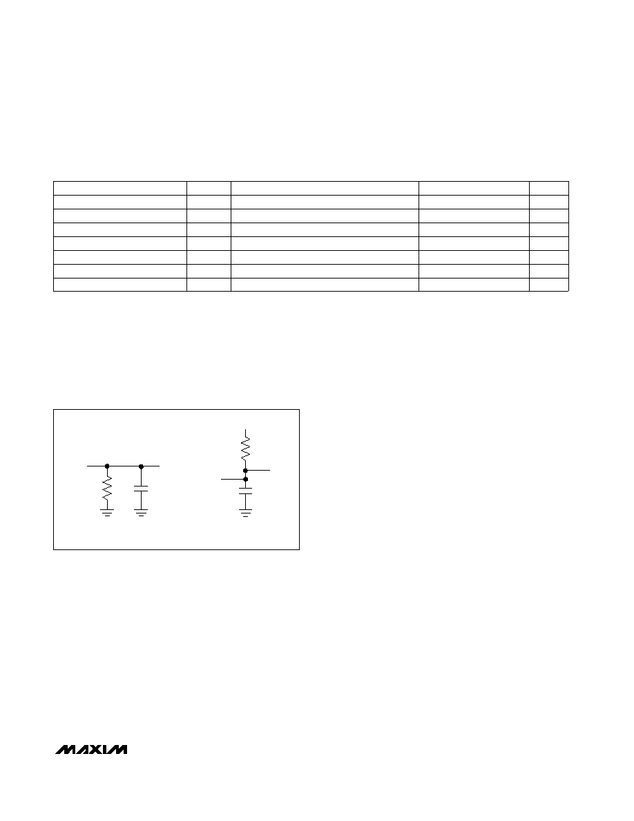
Figure 1. Load Circuits for Enable/Disable Times
tTR
10
40
ns
CLOAD = 20pF, Figure 1
RD Rise to Output Disable
RD Fall to Output Data Valid
tDO
10
50
ns
RD Fall to INT High Delay
tINT1
50
ns
CS Fall to Output Data Valid
tDO2
100
ns
CLOAD = 20pF, Figure 1
tTC
10
60
ns
CLOAD = 20pF, Figure 1
PARAMETER
SYMBOL
MIN
TYP
MAX
UNITS
CONDITIONS
CS Rise to Output Disable
HBEN Rise to Output Data Valid
tDO1
10
50
ns
CLOAD = 20pF, Figure 1
HBEN Fall to Output Data Valid
tDO1
10
80
ns
CLOAD = 20pF, Figure 1
相关PDF资料 |
PDF描述 |
|---|---|
| VE-JWJ-EY | CONVERTER MOD DC/DC 36V 50W |
| MAX1284EVKIT | EVALUATION KIT FOR MAX1284 |
| PMF18WF0 | PROCESSOR MODULE ICE4000 |
| HFI-160808-18NJ | INDUCTOR 1.6X0.8X0.8MM 18NH |
| RCB13DHHD | CONN EDGECARD 26POS DIP .050 SLD |
相关代理商/技术参数 |
参数描述 |
|---|---|
| MAX1293ACEG | 功能描述:模数转换器 - ADC Integrated Circuits (ICs) RoHS:否 制造商:Texas Instruments 通道数量:2 结构:Sigma-Delta 转换速率:125 SPs to 8 KSPs 分辨率:24 bit 输入类型:Differential 信噪比:107 dB 接口类型:SPI 工作电源电压:1.7 V to 3.6 V, 2.7 V to 5.25 V 最大工作温度:+ 85 C 安装风格:SMD/SMT 封装 / 箱体:VQFN-32 |
| MAX1293ACEG+ | 功能描述:模数转换器 - ADC 12-Bit 4Ch 250ksps 3.6V Precision ADC RoHS:否 制造商:Texas Instruments 通道数量:2 结构:Sigma-Delta 转换速率:125 SPs to 8 KSPs 分辨率:24 bit 输入类型:Differential 信噪比:107 dB 接口类型:SPI 工作电源电压:1.7 V to 3.6 V, 2.7 V to 5.25 V 最大工作温度:+ 85 C 安装风格:SMD/SMT 封装 / 箱体:VQFN-32 |
| MAX1293ACEG+T | 功能描述:模数转换器 - ADC 12-Bit 4Ch 250ksps 3.6V Precision ADC RoHS:否 制造商:Texas Instruments 通道数量:2 结构:Sigma-Delta 转换速率:125 SPs to 8 KSPs 分辨率:24 bit 输入类型:Differential 信噪比:107 dB 接口类型:SPI 工作电源电压:1.7 V to 3.6 V, 2.7 V to 5.25 V 最大工作温度:+ 85 C 安装风格:SMD/SMT 封装 / 箱体:VQFN-32 |
| MAX1293ACEG-T | 功能描述:模数转换器 - ADC RoHS:否 制造商:Texas Instruments 通道数量:2 结构:Sigma-Delta 转换速率:125 SPs to 8 KSPs 分辨率:24 bit 输入类型:Differential 信噪比:107 dB 接口类型:SPI 工作电源电压:1.7 V to 3.6 V, 2.7 V to 5.25 V 最大工作温度:+ 85 C 安装风格:SMD/SMT 封装 / 箱体:VQFN-32 |
| MAX1293AEEG | 功能描述:模数转换器 - ADC RoHS:否 制造商:Texas Instruments 通道数量:2 结构:Sigma-Delta 转换速率:125 SPs to 8 KSPs 分辨率:24 bit 输入类型:Differential 信噪比:107 dB 接口类型:SPI 工作电源电压:1.7 V to 3.6 V, 2.7 V to 5.25 V 最大工作温度:+ 85 C 安装风格:SMD/SMT 封装 / 箱体:VQFN-32 |
发布紧急采购,3分钟左右您将得到回复。