- 您现在的位置:买卖IC网 > PDF目录9885 > MAX1300AEUG+T (Maxim Integrated Products)IC ADC 16BIT SRL 115KSPS 24TSSOP PDF资料下载
参数资料
| 型号: | MAX1300AEUG+T |
| 厂商: | Maxim Integrated Products |
| 文件页数: | 17/31页 |
| 文件大小: | 0K |
| 描述: | IC ADC 16BIT SRL 115KSPS 24TSSOP |
| 产品培训模块: | Obsolescence Mitigation Program |
| 标准包装: | 2,500 |
| 位数: | 16 |
| 采样率(每秒): | 115k |
| 数据接口: | MICROWIRE?,QSPI?,串行,SPI? |
| 转换器数目: | 1 |
| 功率耗散(最大): | 976mW |
| 电压电源: | 模拟和数字 |
| 工作温度: | -40°C ~ 85°C |
| 安装类型: | 表面贴装 |
| 封装/外壳: | 24-TSSOP(0.173",4.40mm 宽) |
| 供应商设备封装: | 24-TSSOP |
| 包装: | 带卷 (TR) |
| 输入数目和类型: | 8 个单端,单极;8 个单端,双极;4 个差分,双极 |
第1页第2页第3页第4页第5页第6页第7页第8页第9页第10页第11页第12页第13页第14页第15页第16页当前第17页第18页第19页第20页第21页第22页第23页第24页第25页第26页第27页第28页第29页第30页第31页
MAX1300/MAX1301
External Acquisition Mode (Mode 1)
The slowest maximum throughput rate is achieved with
the external acquisition method. SCLK controls the
acquisition of the analog signal in external acquisition
mode, facilitating precise control over when the analog
signal is captured. The internal clock controls the con-
version of the analog input voltage. The analog input
sampling instant is at the falling edge of the 16th SCLK
(Figure 3).
For the external acquisition mode, CS must remain low
for the first 15 clock cycles and the rise on or after the
falling edge of the 16th SCLK cycle as shown in Figure
3. For optimal performance, idle DIN and SCLK during
the conversion. With careful board layout, transitions at
DIN and SCLK during the conversion have a minimal
impact on the conversion result.
After the conversion is complete, SSTRB asserts high
and CS can be brought low to read the conversion
result. SSTRB returns low on the rising SCLK edge of
the subsequent start bit.
Internal Clock Mode (Mode 2)
In internal clock mode, the internal clock controls both
acquisition and conversion of the analog signal. The inter-
nal clock starts approximately 100ns to 400ns after the
falling edge of the eighth SCLK and has a rate of about
4.5MHz. The analog input sampling instant occurs at the
falling edge of the 11th internal clock signal (Figure 4).
For the internal clock mode, CS must remain low for the
first seven SCLK cycles and then rise on or after the
falling edge of the eighth SCLK cycle. After the conver-
sion is complete, SSTRB asserts high and CS can be
brought low to read the conversion result. SSTRB returns
low on the rising SCLK edge of the subsequent start bit.
Reset (Mode 4)
As shown in Table 8, set M[2:0] = 100 to reset the
MAX1300/MAX1301 to its default conditions. The default
conditions are full power operation with each channel
configured for ±3 x VREF, bipolar, single-ended conver-
sions using external clock mode (mode 0).
Partial Power-Down Mode (Mode 6)
As shown in Table 8, when M[2:0] = 110, the device
enters partial power-down mode. In partial power-
down, all analog portions of the device are powered
down except for the reference voltage generator and
bias supplies.
To exit partial power-down, change the mode by issu-
ing one of the following mode-control bytes (see the
Mode Control section):
External-Clock-Mode Control Byte
External-Acquisition-Mode Control Byte
Internal-Clock-Mode Control Byte
Reset Byte
Full Power-Down-Mode Control Byte
This prevents the MAX1300/MAX1301 from inadvertent-
ly exiting partial power-down mode because of a CS
glitch in a noisy digital environment.
Full Power-Down Mode (Mode 7)
When M[2:0] = 111, the device enters full power-down
mode and the total supply current falls to 1A (typ). In
full power-down, all analog portions of the device are
powered down. When using the internal reference,
upon exiting full power-down mode, allow 10ms for the
internal reference voltage to stabilize prior to initiating a
conversion.
To exit full power-down, change the mode by issuing
one of the following mode-control bytes (see the
Mode
Control section):
External-Clock-Mode Control Byte
8- and 4-Channel, ±3 x VREF Multirange Inputs,
Serial 16-Bit ADCs
24
______________________________________________________________________________________
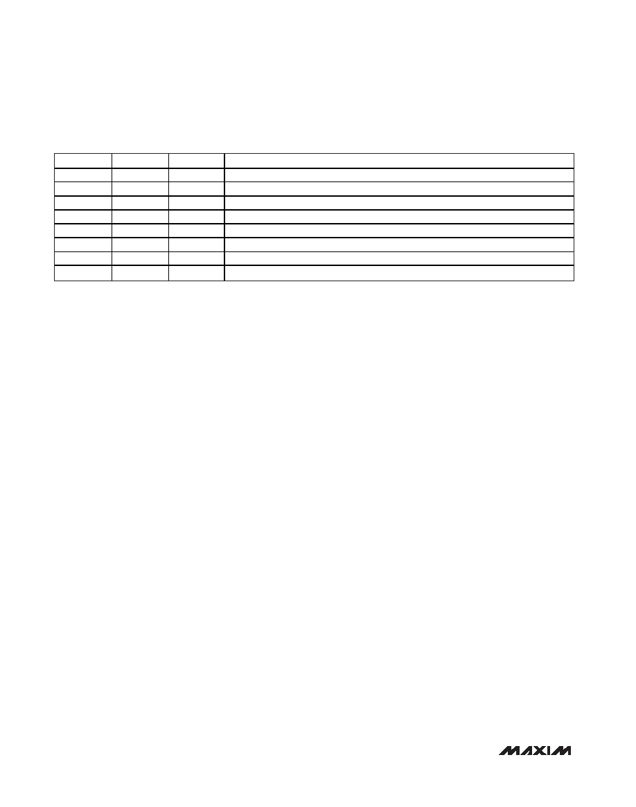
M2
M1
M0
MODE
0
External Clock (DEFAULT)
0
1
External Acquisition
0
1
0
Internal Clock
0
1
Reserved
1
0
Reset
1
0
1
Reserved
1
0
Partial Power-Down
1
Full Power-Down
Table 8. Mode-Control Bits M[2:0]
相关PDF资料 |
PDF描述 |
|---|---|
| MAX1302AEUG+T | IC ADC 16BIT SRL 115KSPS 24TSSOP |
| VI-2WH-MX-F4 | CONVERTER MOD DC/DC 52V 75W |
| PI90LV027AWE | IC DUAL LVDS LINE DRIVER 8-SOIC |
| MAX1203BCAP+ | IC ADC 12BIT 8CH 20-SSOP |
| VE-J33-MX-F3 | CONVERTER MOD DC/DC 24V 75W |
相关代理商/技术参数 |
参数描述 |
|---|---|
| MAX1300AEVKIT# | 功能描述:数据转换 IC 开发工具 MAX1300 Eval Kit RoHS:否 制造商:Texas Instruments 产品:Demonstration Kits 类型:ADC 工具用于评估:ADS130E08 接口类型:SPI 工作电源电压:- 6 V to + 6 V |
| MAX1300BEUG+ | 功能描述:模数转换器 - ADC 16-Bit 8Ch 115ksps 4.136V Precision ADC RoHS:否 制造商:Texas Instruments 通道数量:2 结构:Sigma-Delta 转换速率:125 SPs to 8 KSPs 分辨率:24 bit 输入类型:Differential 信噪比:107 dB 接口类型:SPI 工作电源电压:1.7 V to 3.6 V, 2.7 V to 5.25 V 最大工作温度:+ 85 C 安装风格:SMD/SMT 封装 / 箱体:VQFN-32 |
| MAX1300BEUG+T | 功能描述:模数转换器 - ADC 16-Bit 8Ch 115ksps 4.136V Precision ADC RoHS:否 制造商:Texas Instruments 通道数量:2 结构:Sigma-Delta 转换速率:125 SPs to 8 KSPs 分辨率:24 bit 输入类型:Differential 信噪比:107 dB 接口类型:SPI 工作电源电压:1.7 V to 3.6 V, 2.7 V to 5.25 V 最大工作温度:+ 85 C 安装风格:SMD/SMT 封装 / 箱体:VQFN-32 |
| MAX1300EVKIT+ | 功能描述:数据转换 IC 开发工具 MAX1300 Eval Kit RoHS:否 制造商:Texas Instruments 产品:Demonstration Kits 类型:ADC 工具用于评估:ADS130E08 接口类型:SPI 工作电源电压:- 6 V to + 6 V |
| MAX13013EBT | 制造商:Rochester Electronics LLC 功能描述: 制造商:Maxim Integrated Products 功能描述: |
发布紧急采购,3分钟左右您将得到回复。