- 您现在的位置:买卖IC网 > PDF目录8943 > MAX13030EEBE+T (Maxim Integrated Products)IC TRANSLATOR LL 6CH 16UCSP PDF资料下载
参数资料
| 型号: | MAX13030EEBE+T |
| 厂商: | Maxim Integrated Products |
| 文件页数: | 4/18页 |
| 文件大小: | 0K |
| 描述: | IC TRANSLATOR LL 6CH 16UCSP |
| 产品培训模块: | Lead (SnPb) Finish for COTS Obsolescence Mitigation Program |
| 标准包装: | 1 |
| 逻辑功能: | 变换器,双向 |
| 位数: | 6 |
| 输入类型: | 逻辑 |
| 输出类型: | 逻辑 |
| 数据速率: | 100Mbps |
| 通道数: | 6 |
| 输出/通道数目: | 1 |
| 差分 - 输入:输出: | 无/无 |
| 传输延迟(最大): | 6.5ns |
| 电源电压: | 2.2 V ~ 3.6 V |
| 工作温度: | -40°C ~ 85°C |
| 封装/外壳: | 16-WFBGA,CSPBGA |
| 供应商设备封装: | 16-UCSP(2x2) |
| 包装: | 标准包装 |
| 其它名称: | MAX13030EEBE+TDKR |
MAX13030E–MAX13035E
Detailed Description
The MAX13030E–MAX13035E 6-channel, bidirectional
level translators provide the level shifting necessary for
100Mbps data transfer in multivoltage systems. The
MAX13030E–MAX13035E are ideally suited for memory
card level translation, as well as generic level translation
in systems with six channels. Externally applied volt-
ages, VCC and VL, set the logic levels on either side of
the device. Logic signals present on the VL side of the
device appear as a higher voltage logic signal on the
VCC side of the device, and vice versa. The MAX13035E
features a CLK_RET output that returns the same clock
signal applied to the CLK_VL input.
The MAX13030E–MAX13035E operate at full speed
with external drivers that source as little as 4mA output
current. Each I/O channel is pulled up to VCC or VL by
an internal 30A current source, allowing the
MAX13030E–MAX13035E to be driven by either push-
pull or open-drain drivers.
The MAX13030E–MAX13034E feature an enable (EN)
input that places the device into a low-power shutdown
mode when driven low. The MAX13030E–MAX13035E
features an automatic shutdown mode that disables the
part when VCC is less than VL. The state of I/O VCC_ and
I/O VL_ during shutdown is chosen by selecting the
appropriate part version (see
Ordering Information/
Selector Guide).
The MAX13030E–MAX13035E accept VCC voltages from
+2.2V to +3.6V and VL voltages from +1.62V to +3.2V.
Level Translation
For proper operation, ensure that +2.2V ≤ VCC ≤ +3.6V,
and +1.62V ≤ VL ≤ VCC - 0.2V. When power is supplied to
VL while VCC is either missing or less than VL,
the MAX13030E–MAX13035E automatically enters a
low- power mode. In addition, the MAX13030E–
MAX13034E enters a low-power mode if EN = 0V. This
allows VCC to be disconnected and still have a known
state on I/O VL_. The maximum data rate depends heavily
on the load capacitance (see the
Typical Operating
Characteristics Rise/Fall Times), output impedance of the
driver, and the operating voltage range.
Input Driver Requirements
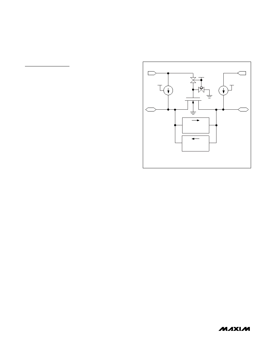
The MAX13030E–MAX13035E architecture is based on
an nMOS pass gate and output accelerator stages (see
Figure 6). Output accelerator stages are always in tri-
state mode except when there is a transition on any of
the translators on the input side, either I/O VL_, CLK_VL,
I/O VCC_, or CLK_VCC. A short pulse is then generated
during which the output accelerator stages become
active and charge/discharge the capacitances at the
I/Os. Due to its architecture, both input stages become
active during the one-shot pulse. This can lead to some
current feeding into the external source that is driving the
translator. However, this behavior helps to speed up the
transition on the driven side.
The MAX13030E–MAX13035E have internal current
sources capable of sourcing 30A to pullup the I/O
lines. These internal pullup current sources allow the
inputs to be driven with open-drain drivers, as well as
push-pull drivers. It is not recommended to use exter-
nal pullup resistors on the I/O lines. The architecture of
the MAX13030E–MAX13035E permit either side to be
driven with a minimum of 4mA drivers or larger.
Output Load Requirements
The MAX13030E–MAX13035E I/O are designed to drive
CMOS inputs. Do not load the I/O lines with a resistive
load less than 25kΩ and do not place an RC circuit at
the input of these devices to slow down the edges. If a
slower rise/fall time is required, refer to the MAX3000E/
MAX3001E logic-level translator datasheet. For I2C
level translation, refer to the MAX3372E–MAX3379E/
MAX3390E–MAX3393E datasheet.
Shutdown Mode
The MAX13030E–MAX13034E feature an enable (EN)
input that places the device into a low-power shutdown
mode when driven low. The MAX13030E–MAX13035E
features an automatic shutdown mode that disables the
part when VCC is missing or less than VL.
6-Channel High-Speed Logic-Level Translators
12
______________________________________________________________________________________
30
μA
VL
ENABLE
VCC
30
μA
BOOST
CIRCUIT
I/O VL_
VL
VCC
BOOST
CIRCUIT
VCC
VL
I/O VCC_
NOTES: 1) THE MAX13030E–MAX13034E ARE ENABLED WHEN
VL < VCC - 0.2V AND EN = VL.
2) THE MAX13035E IS ENABLED WHEN VL < VCC - 0.2V.
Figure 6. Simplified Functional Diagram for One I/O Line
相关PDF资料 |
PDF描述 |
|---|---|
| VI-J1Y-MZ-F1 | CONVERTER MOD DC/DC 3.3V 16.5W |
| VE-B0F-MY-F3 | CONVERTER MOD DC/DC 72V 50W |
| VI-J0J-MZ-F2 | CONVERTER MOD DC/DC 36V 25W |
| MAX13003EEUE+ | IC LEVEL TRANS 6CH 16-TSSOP |
| VE-B0F-MY-F2 | CONVERTER MOD DC/DC 72V 50W |
相关代理商/技术参数 |
参数描述 |
|---|---|
| MAX13030EETE+ | 功能描述:转换 - 电压电平 6Ch High-Speed RoHS:否 制造商:Micrel 类型:CML/LVDS/LVPECL to LVCMOS/LVTTL 传播延迟时间:1.9 ns 电源电流:14 mA 电源电压-最大:3.6 V 电源电压-最小:3 V 最大工作温度:+ 85 C 安装风格:SMD/SMT 封装 / 箱体:MLF-8 |
| MAX13030EETE+T | 功能描述:转换 - 电压电平 6Ch High-Speed RoHS:否 制造商:Micrel 类型:CML/LVDS/LVPECL to LVCMOS/LVTTL 传播延迟时间:1.9 ns 电源电流:14 mA 电源电压-最大:3.6 V 电源电压-最小:3 V 最大工作温度:+ 85 C 安装风格:SMD/SMT 封装 / 箱体:MLF-8 |
| MAX13031E | 功能描述:模数转换器 - ADC RoHS:否 制造商:Texas Instruments 通道数量:2 结构:Sigma-Delta 转换速率:125 SPs to 8 KSPs 分辨率:24 bit 输入类型:Differential 信噪比:107 dB 接口类型:SPI 工作电源电压:1.7 V to 3.6 V, 2.7 V to 5.25 V 最大工作温度:+ 85 C 安装风格:SMD/SMT 封装 / 箱体:VQFN-32 |
| MAX13032EEBE+ | 制造商:Maxim Integrated Products 功能描述: 制造商:Rochester Electronics LLC 功能描述: |
| MAX13032EEBE+T | 功能描述:转换 - 电压电平 6Ch High-Speed RoHS:否 制造商:Micrel 类型:CML/LVDS/LVPECL to LVCMOS/LVTTL 传播延迟时间:1.9 ns 电源电流:14 mA 电源电压-最大:3.6 V 电源电压-最小:3 V 最大工作温度:+ 85 C 安装风格:SMD/SMT 封装 / 箱体:MLF-8 |
发布紧急采购,3分钟左右您将得到回复。