- 您现在的位置:买卖IC网 > PDF目录9906 > MAX1303BEUP+T (Maxim Integrated Products)IC ADC 16BIT MULT RANGE 20TSSOP PDF资料下载
参数资料
| 型号: | MAX1303BEUP+T |
| 厂商: | Maxim Integrated Products |
| 文件页数: | 4/29页 |
| 文件大小: | 0K |
| 描述: | IC ADC 16BIT MULT RANGE 20TSSOP |
| 标准包装: | 2,500 |
| 位数: | 16 |
| 采样率(每秒): | 115k |
| 数据接口: | 串行 |
| 转换器数目: | 1 |
| 功率耗散(最大): | 105.5mW |
| 电压电源: | 模拟和数字 |
| 工作温度: | -40°C ~ 85°C |
| 安装类型: | 表面贴装 |
| 封装/外壳: | 20-TSSOP(0.173",4.40mm 宽) |
| 供应商设备封装: | 20-TSSOP |
| 包装: | 带卷 (TR) |
| 输入数目和类型: | 4 个单端,单极;4 个单端,双极;2 个差分,双极 |
第1页第2页第3页当前第4页第5页第6页第7页第8页第9页第10页第11页第12页第13页第14页第15页第16页第17页第18页第19页第20页第21页第22页第23页第24页第25页第26页第27页第28页第29页
MAX1303
4-Channel, ±VREF Multirange Inputs,
Serial 16-Bit ADC
12
______________________________________________________________________________________
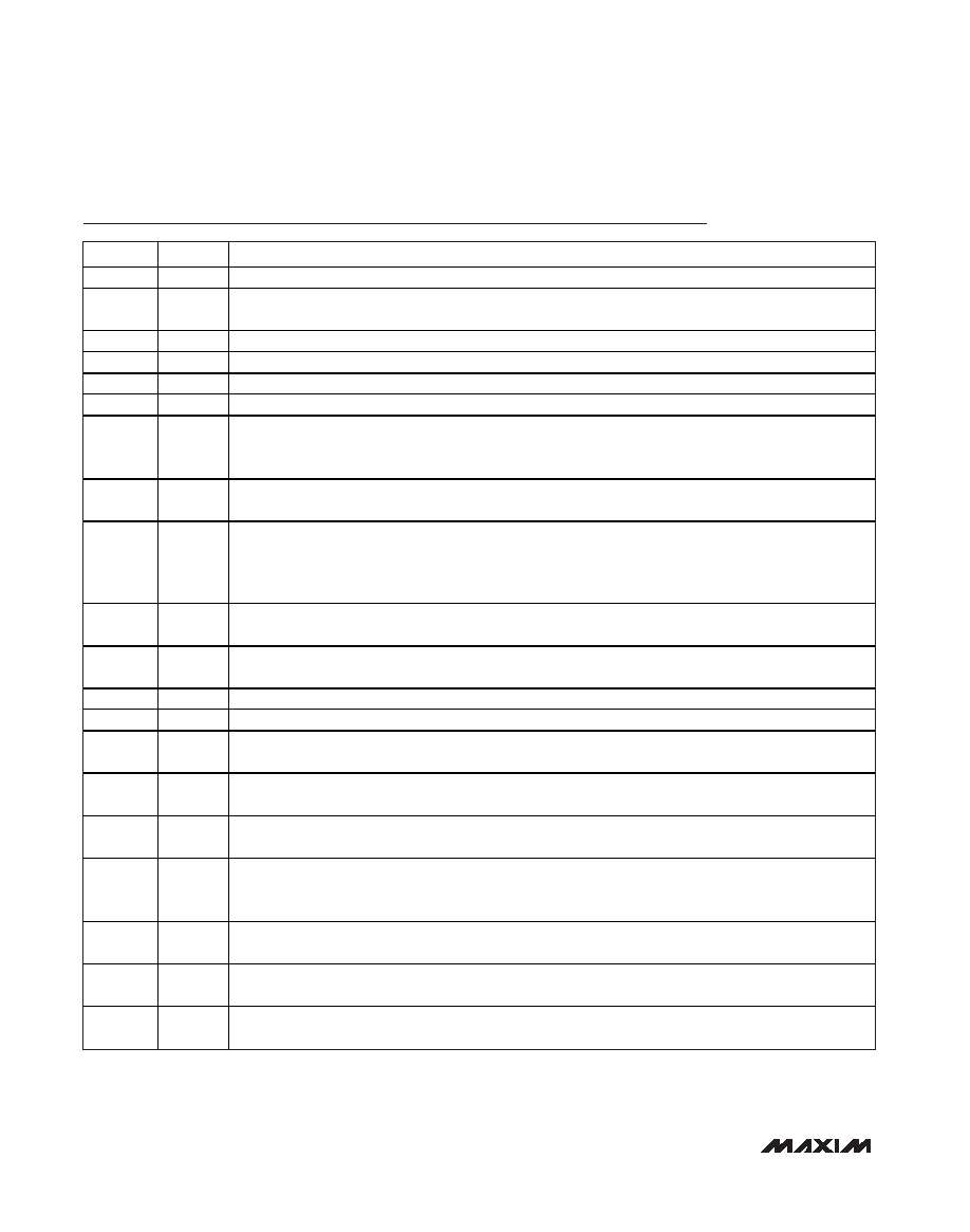
Pin Description
PIN
NAME
FUNCTION
1
AGND1
Analog Ground 1. DGND, DGNDO, AGND3, AGND2, and AGND1 must be connected together.
2
AVDD1
Analog Supply Voltage 1. Connect AVDD1 to a +4.75V to +5.25V power-supply voltage. Bypass AVDD1 to
AGND1 with a 0.1F capacitor.
3
CH0
Analog Input Channel 0
4
CH1
Analog Input Channel 1
5
CH2
Analog Input Channel 2
6
CH3
Analog Input Channel 3
7
CS
Active-Low Chip-Select Input. When CS is low, data is clocked into the device from DIN on the rising edge
of SCLK. With CS low, data is clocked out of DOUT on the falling edge of SCLK. When CS is high, activity
on SCLK and DIN is ignored and DOUT is high impedance.
8DIN
Serial Data Input. When CS is low, data is clocked in on the rising edge of SCLK. When CS is high,
transitions on DIN are ignored.
9
SSTRB
Serial-Strobe Output. When using the internal clock, SSTRB rising edge transitions indicate that data is
ready to be read from the device. When operating in external clock mode, SSTRB is always low. SSTRB
does not tri-state, regardless of the state of CS, and therefore requires
a dedicated I/O line.
10
SCLK
Serial Clock Input. When CS is low, transitions on SCLK clock data into DIN and out of DOUT. When CS is
high, transitions on SCLK are ignored.
11
DOUT
Serial Data Output. When CS is low, data is clocked out of DOUT with each falling SCLK transition. When
CS is high, DOUT is high impedance.
12
DGNDO
Digital I/O Ground. DGND, DGNDO, AGND3, AGND2, and AGND1 must be connected together.
13
DGND
Digital Ground. DGND, DGNDO, AGND3, AGND2, and AGND1 must be connected together.
14
DVDDO
Digital I/O Supply Voltage Input. Connect DVDDO to a +2.7V to +5.25V power-supply voltage. Bypass
DVDDO to DGNDO with a 0.1F capacitor.
15
DVDD
Digital-Supply Voltage Input. Connect DVDD to a +4.75V to +5.25V power-supply voltage. Bypass DVDD
to DGND with a 0.1F capacitor.
16
REFCAP
Bandgap-Voltage Bypass Node. For external reference operation, connect REFCAP to AVDD. For internal
reference operation, bypass REFCAP with a 0.01F capacitor to AGND1 (VREFCAP
≈ 4.096V).
17
REF
Reference-Buffer Output/ADC Reference Input. For external reference operation, apply an external
reference voltage from 3.800V to 4.136V to REF. For internal reference operation, bypassing REF with a
1F capacitor to AGND1 sets VREF = 4.096V ±1%.
18
AGND3
Analog Signal Ground 3. AGND3 is the ADC negative reference potential. Connect AGND3 to AGND1.
DGND, DGNDO, AGND3, AGND2, and AGND1 must be connected together.
19
AVDD2
Analog Supply Voltage 2. Connect AVDD2 to a +4.75V to +5.25V power-supply voltage. Bypass AVDD2 to
AGND2 with a 0.1F capacitor.
20
AGND2
Analog Ground 2. This ground carries approximately five times more current than AGND1. DGND,
DGNDO, AGND3, AGND2, and AGND1 must be connected together.
相关PDF资料 |
PDF描述 |
|---|---|
| VE-J2H-MX-F3 | CONVERTER MOD DC/DC 52V 75W |
| VE-J2H-MX-F2 | CONVERTER MOD DC/DC 52V 75W |
| VI-JWM-MW-B1 | CONVERTER MOD DC/DC 10V 100W |
| MAX144AEUA+T | IC ADC 12BIT 108KSPS 8-UMAX |
| IDT723666L12PF | IC FIFO SYNC 8192X36 128QFP |
相关代理商/技术参数 |
参数描述 |
|---|---|
| MAX13041ASD/V+ | 功能描述:CAN 接口集成电路 80V Fault-Protected High-Speed RoHS:否 制造商:Texas Instruments 类型:Transceivers 工作电源电压:5 V 电源电流: 工作温度范围:- 40 C to + 85 C 封装 / 箱体:SOIC-8 封装:Tube |
| MAX13041ASD/V+T | 功能描述:CAN 接口集成电路 80V Fault-Protected High-Speed RoHS:否 制造商:Texas Instruments 类型:Transceivers 工作电源电压:5 V 电源电流: 工作温度范围:- 40 C to + 85 C 封装 / 箱体:SOIC-8 封装:Tube |
| MAX13041ASD+ | 功能描述:CAN 接口集成电路 80V Fault-Protected High-Speed RoHS:否 制造商:Texas Instruments 类型:Transceivers 工作电源电压:5 V 电源电流: 工作温度范围:- 40 C to + 85 C 封装 / 箱体:SOIC-8 封装:Tube |
| MAX13041ASD+T | 功能描述:CAN 接口集成电路 80V Fault-Protected High-Speed RoHS:否 制造商:Texas Instruments 类型:Transceivers 工作电源电压:5 V 电源电流: 工作温度范围:- 40 C to + 85 C 封装 / 箱体:SOIC-8 封装:Tube |
| MAX13042EEBC+ | 制造商:Maxim Integrated Products 功能描述: |
发布紧急采购,3分钟左右您将得到回复。