- 您现在的位置:买卖IC网 > PDF目录3709 > MAX13202EALT+T (Maxim Integrated Products)IC ESD PROTECT 2CH 6-UDFN PDF资料下载
参数资料
| 型号: | MAX13202EALT+T |
| 厂商: | Maxim Integrated Products |
| 文件页数: | 4/9页 |
| 文件大小: | 0K |
| 描述: | IC ESD PROTECT 2CH 6-UDFN |
| 产品培训模块: | Lead (SnPb) Finish for COTS Obsolescence Mitigation Program |
| 标准包装: | 1 |
| 电极标记: | 2 通道阵列 - 单向 |
| 安装类型: | 表面贴装 |
| 封装/外壳: | 6-WFDFN |
| 供应商设备封装: | 6-uDFN(1.5x1.0) |
| 包装: | 标准包装 |
| 产品目录页面: | 1424 (CN2011-ZH PDF) |
| 其它名称: | MAX13202EALT+TDKR |
�� �
�
�2-/4-/6-/8-Channel,� ±30kV� ESD� Protectors� in� μDFN�
�V� C� =� ?� ?� V� F� (� D� 2� )� +� ?� L� 1� x�
�?� +� ?� L� 3� x�
�d� (� I� ESD� )� ?� ?�
�?� ?�
�?� ?�
�Detailed� Description�
�The� MAX13202E/MAX13204E/MAX13206E/MAX13208E�
�are� diode� arrays� designed� to� protect� sensitive� electron-�
�?� ?�
�?� ?�
�d� (� I� ESD� )� ?� ?�
�dt� ?� ?�
�dt�
�ics� against� damage� resulting� from� ESD� conditions� or�
�transient� voltages.� The� low� input� capacitance� makes�
�these� devices� ideal� for� high-speed� data� lines.� The�
�MAX13202E/MAX13204E/MAX13206E/MAX13208E�
�protect� two,� four,� six,� and� eight� channels,� respectively.�
�The� MAX13202E/MAX13204E/MAX13206E/MAX13208E�
�are� designed� to� work� in� conjunction� with� a� device’s�
�intrinsic� ESD� protection.� The� MAX13202E/MAX13204E/�
�MAX13206E/MAX13208E� limit� the� excursion� of� the� ESD�
�event� to� below� ±25V� peak� voltage� when� subjected� to� the�
�where� I� ESD� is� the� ESD� current� pulse.�
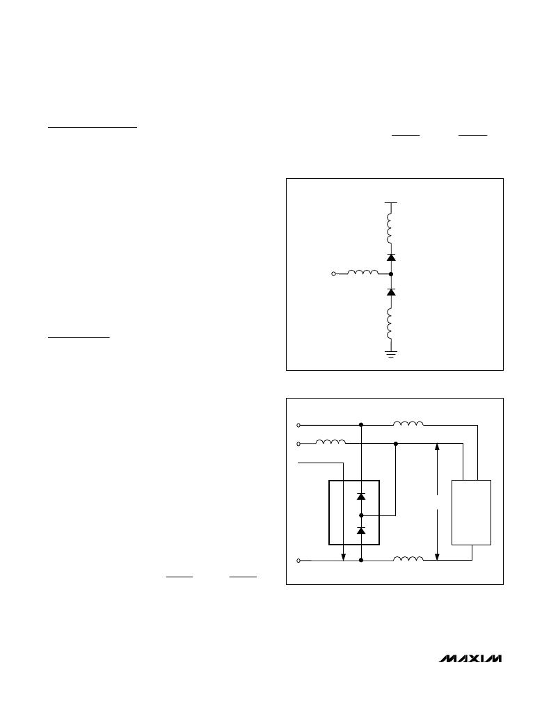
�POSITIVE� SUPPLY� RAIL�
�L2�
�Human� Body� Model� waveform.� When� subjected� to� the�
�IEC� 61000-4-2� waveform,� the� peak� voltage� is� limited� to�
�±80V� (Contact� Discharge)� and� ±120V� (Air-Gap�
�Discharge).� The� device� that� is� being� protected� by� the�
�MAX13202E/MAX13204E/� MAX13206E/MAX13208E�
�PROTECTED�
�LINE�
�L1�
�D1�
�I/O_�
�D2�
�must� be� able� to� withstand� these� peak� voltages� plus� any�
�additional� voltage� generated� by� the� parasitic� board.�
�Applications� Information�
�Design� Considerations�
�Maximum� protection� against� ESD� damage� results� from�
�proper� board� layout� (see� the� Layout� Recommendations�
�section� and� Figure� 2).� A� good� layout� reduces� the� para-�
�sitic� series� inductance� on� the� ground� line,� supply� line,�
�and� protected� signal� lines.�
�L3�
�GROUND� RAIL�
�Figure� 1.� Parasitic� Series� Inductance�
�The� MAX13202E/MAX13204E/MAX13206E/MAX13208E�
�ESD� diodes� clamp� the� voltage� on� the� protected� lines�
�during� an� ESD� event� and� shunt� the� current� to� GND� or�
�V� CC� .� In� an� ideal� circuit,� the� clamping� voltage,� V� C� ,� is�
�defined� as� the� forward� voltage� drop,� V� F� ,� of� the� protection�
�diode� plus� any� supply� voltage� present� on� the� cathode.�
�For� positive� ESD� pulses:�
�V� CC�
�L1�
�PROTECTED� LINE�
�NEGATIVE� ESD�
�CURRENT�
�L2�
�V� C� =� V� CC� +� V� F�
�For� negative� ESD� pulses:�
�V� C� =� -V� F�
�PULSE�
�PATH� TO�
�GROUND�
�D1�
�I/O_�
�V� C�
�PROTECTED�
�CIRCUIT�
�In� reality,� the� effect� of� the� parasitic� series� inductance�
�on� the� lines� must� also� be� considered� (Figure� 1).�
�D2�
�For� positive� ESD� pulses:�
�GND�
�L3�
�V� C� CC� F� (� D� 1� )� +� ?� L� 1� x�
�=� V�
�+� V�
�?� +� ?� L� 2� x�
�d� (� I� ESD� )� ?�
�?�
�?�
�?�
�?�
�d� (� I� ESD� )� ?� ?�
�dt� ?� ?�
�dt�
�Figure� 2.� Layout� Considerations�
�For� negative� ESD� pulses:�
�4�
�_______________________________________________________________________________________�
�相关PDF资料 |
PDF描述 |
|---|---|
| 1744037-4 | 04P EC PWR.200 CL HDR ASSY VRT |
| 2029167-4 | CONN PLUG 4POS STR NO DRAIN HOLE |
| MMS-103-01-T-SH | CONN RCPT 2MM 3POS SGL HORZ PCB |
| 929836-01-18-RK | CONN HEADER 36POS DUAL .100 TIN |
| 9-103329-0-23 | CONN HEADR BRKWAY .100 23POS R/A |
相关代理商/技术参数 |
参数描述 |
|---|---|
| MAX13204EALT | 制造商:Maxim Integrated Products 功能描述:LOW-CAPACITANCE 4-/6-/8-CHANNEL + - Rail/Tube |
| MAX13204EALT+ | 制造商:Maxim Integrated Products 功能描述: 制造商:Rochester Electronics LLC 功能描述: |
| MAX13204EALT+T | 功能描述:TVS二极管阵列 4Ch ESD Protection Diode Array RoHS:否 制造商:Littelfuse 极性: 通道:4 Channels 击穿电压: 钳位电压:11.5 V 工作电压:2.5 V 峰值浪涌电流:20 A 安装风格:SMD/SMT 端接类型:SMD/SMT 系列: 最小工作温度:- 40 C 最大工作温度:+ 85 C |
| MAX13204EALT-T | 功能描述:TVS二极管阵列 RoHS:否 制造商:Littelfuse 极性: 通道:4 Channels 击穿电压: 钳位电压:11.5 V 工作电压:2.5 V 峰值浪涌电流:20 A 安装风格:SMD/SMT 端接类型:SMD/SMT 系列: 最小工作温度:- 40 C 最大工作温度:+ 85 C |
| MAX13204EELT+ | 制造商:Rochester Electronics LLC 功能描述: 制造商:Maxim Integrated Products 功能描述: |
发布紧急采购,3分钟左右您将得到回复。